Method of manufacturing imprint substrate and imprinting method

a technology of imprint substrate and imprinting method, which is applied in the direction of photomechanical equipment, instruments, originals for photomechanical treatment, etc., can solve the problems of difficult control of the flow direction and the flow degree of the thin film, and achieve the effect of simplifying the manufacturing process of the imprint substra

Active Publication Date: 2009-11-19
SAMSUNG DISPLAY CO LTD
View PDF10 Cites 16 Cited by
  • Summary
  • Abstract
  • Description
  • Claims
  • Application Information

AI Technical Summary

Benefits of technology

[0008]Exemplary embodiments of the present invention provide a method of manufacturing an imprint substrate capable of simplifying the manufacturing process of the imprint substrate.

Problems solved by technology

However, the flow degree and the flow direction of the thin film are not always easily controlled.

Method used


Image

  • Method of manufacturing imprint substrate and imprinting method
  • Method of manufacturing imprint substrate and imprinting method
  • Method of manufacturing imprint substrate and imprinting method

Examples


Embodiment Construction

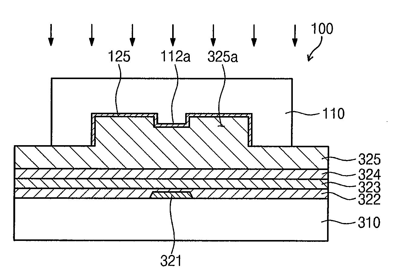
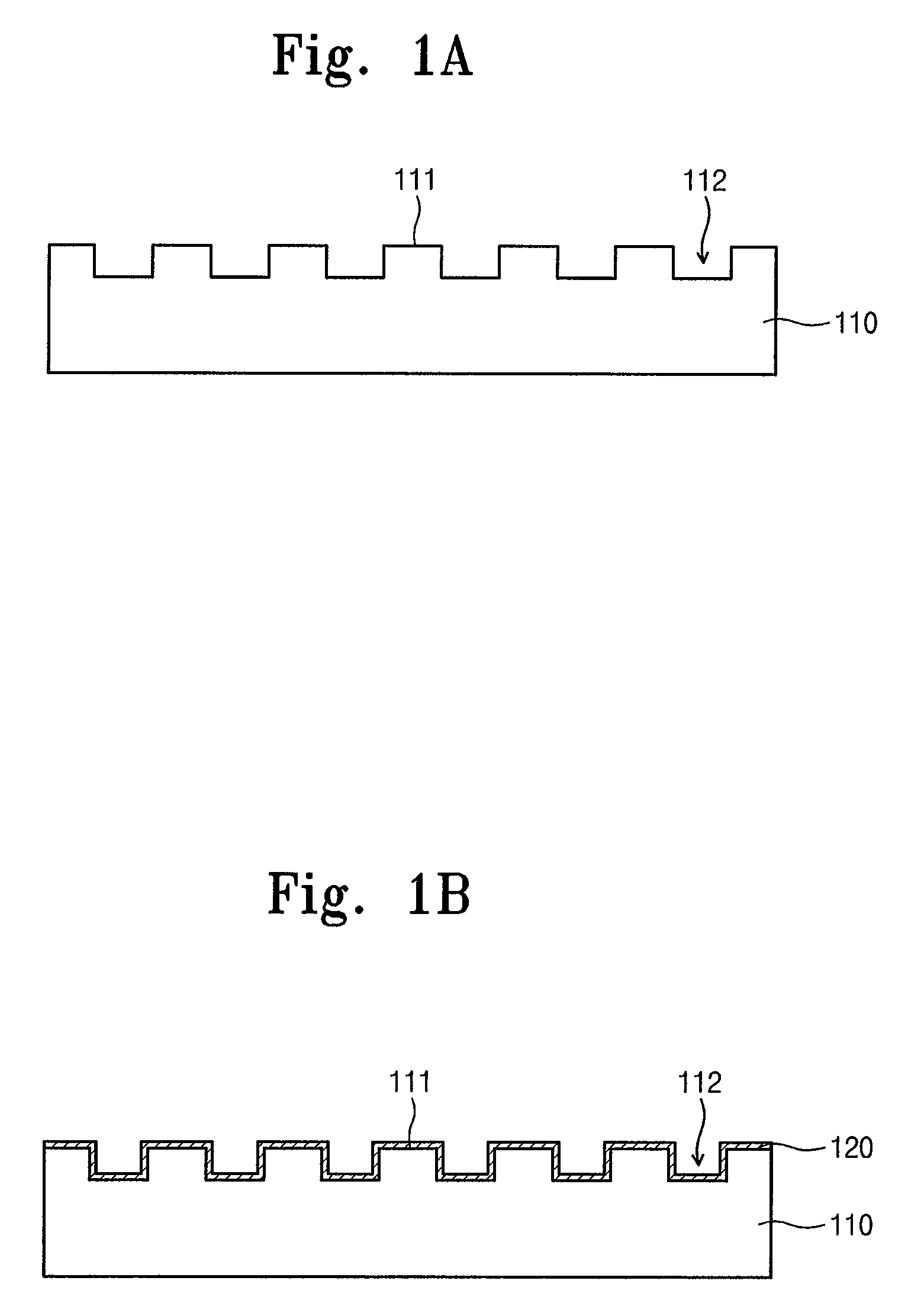
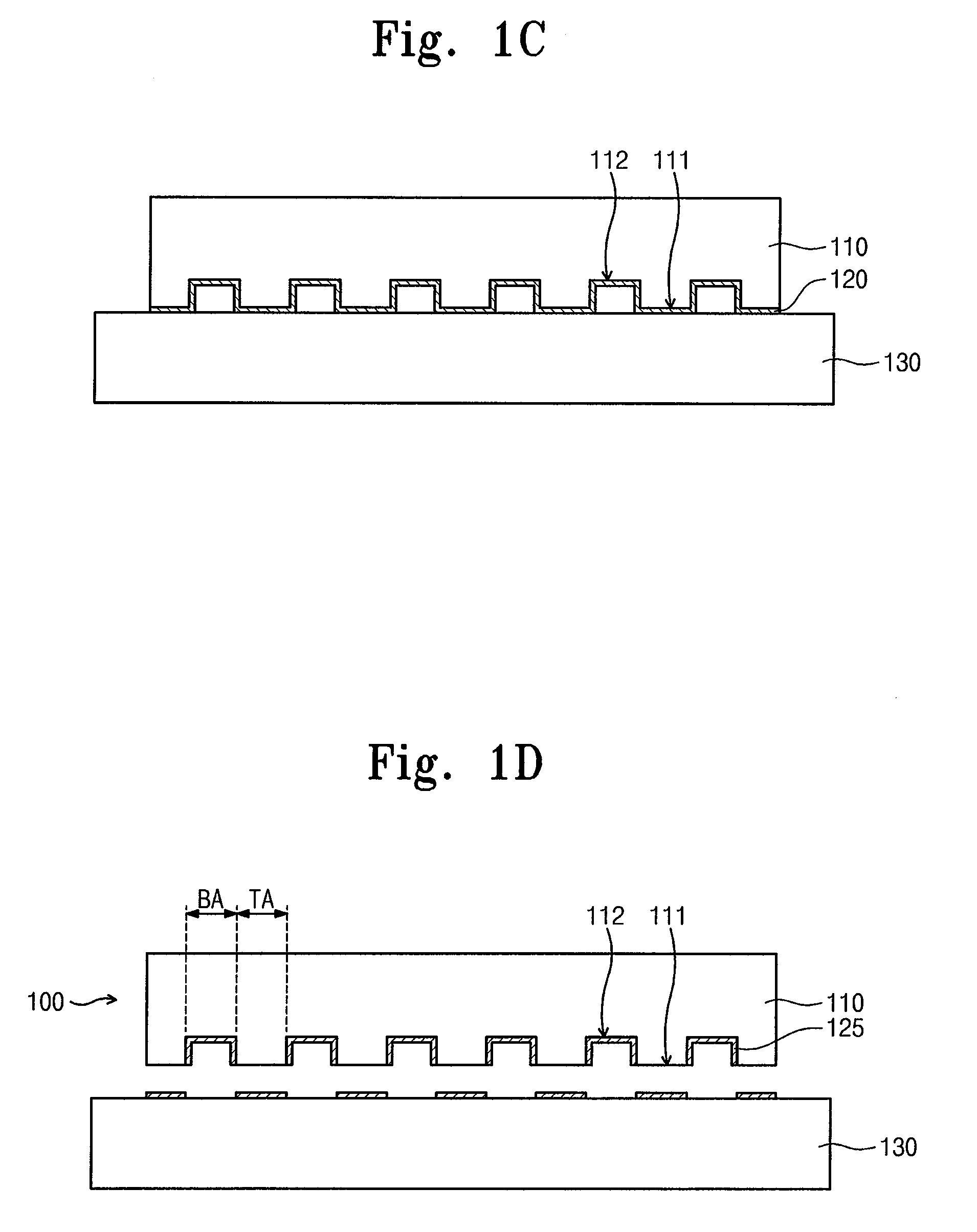
[0017]It will be understood that when an element or layer is referred to as being “on”, “connected to” or “coupled to” another element or layer, it can be directly on, connected or coupled to the other element or layer or intervening elements or layers may be present. In contrast, when an element is referred to as being “directly on,”“directly connected to” or “directly coupled to” another element or layer, there are no intervening elements or layers present. Like numbers refer to like elements throughout. As used herein, the term “and / or” includes any and all combinations of one or more of the associated listed items.

[0018]It will be understood that, although the terms first, second, etc. may be used herein to describe various elements, components, regions, layers and / or sections, these elements, components, regions, layers and / or sections should not be limited by these terms. These terms are only used to distinguish one element, component, region, layer or section from another reg...


PUM

PropertyMeasurementUnit
adhesiveaaaaaaaaaa
flow rateaaaaaaaaaa
thicknessaaaaaaaaaa

Abstract

In a method of manufacturing an imprint substrate, a concave pattern, which is recessed, is formed on a top surface of the mold substrate. A light blocking layer is formed on the concave pattern and the top surface of the mold substrate. After bonding an adhesive substrate to the mold substrate such that the adhesive substrate faces the mold substrate, the adhesive substrate is separated from the mold substrate, so that the light blocking layer on the top surface is removed from the mold substrate. An imprint substrate having the light blocking layer only on the concave pattern is formed.

Description

CROSS-REFERENCE TO RELATED APPLICATION[0001]This application claims priority to Korean Patent Application No. 2008-44846 filed on May 15, 2008, the contents of which are herein incorporated by reference in their entirety.BACKGROUND[0002]1. Field of the Invention[0003]The present invention relates to semiconductor device fabrication. More particularly, the present invention relates to a method of manufacturing an imprint substrate and an imprinting method.[0004]2. Description of the Related Art[0005]Generally, the forming of nano-scale micro patterns is performed via nano-imprint technology. This nano-imprint technology is a lithography technology useful to form a device, such as a liquid crystal display panel or a semiconductor chip, stacked with thin films having micro patterns.[0006]In current nano-imprint technology, after loading a patterned mold substrate on a processing substrate having a thin film thereon, the mold substrate is pressed against the process substrate, so that t...

Claims


Application Information

Patent Timeline
Patent Type & Authority Applications(United States)
IPC IPC(8): H01L21/762B32B38/10G03F7/20
CPCB82Y10/00G03F7/0002B82Y40/00
Inventor HONG, PIL-SOON
Owner SAMSUNG DISPLAY CO LTD
Why Eureka
Try Eureka