

Method for critical dimension shrink using conformal pecvd films
- Summary
- Abstract
- Description
- Claims
- Application Information
AI Technical Summary
Benefits of technology
Problems solved by technology
Method used
Image

Examples
Embodiment Construction
[0023]The invention generally relates to methods of processing a substrate. Embodiments of the invention provide methods of forming recesses or vias in substrates, wherein the recesses or vias have smaller critical dimensions than would be obtained through conventional lithographic processes.
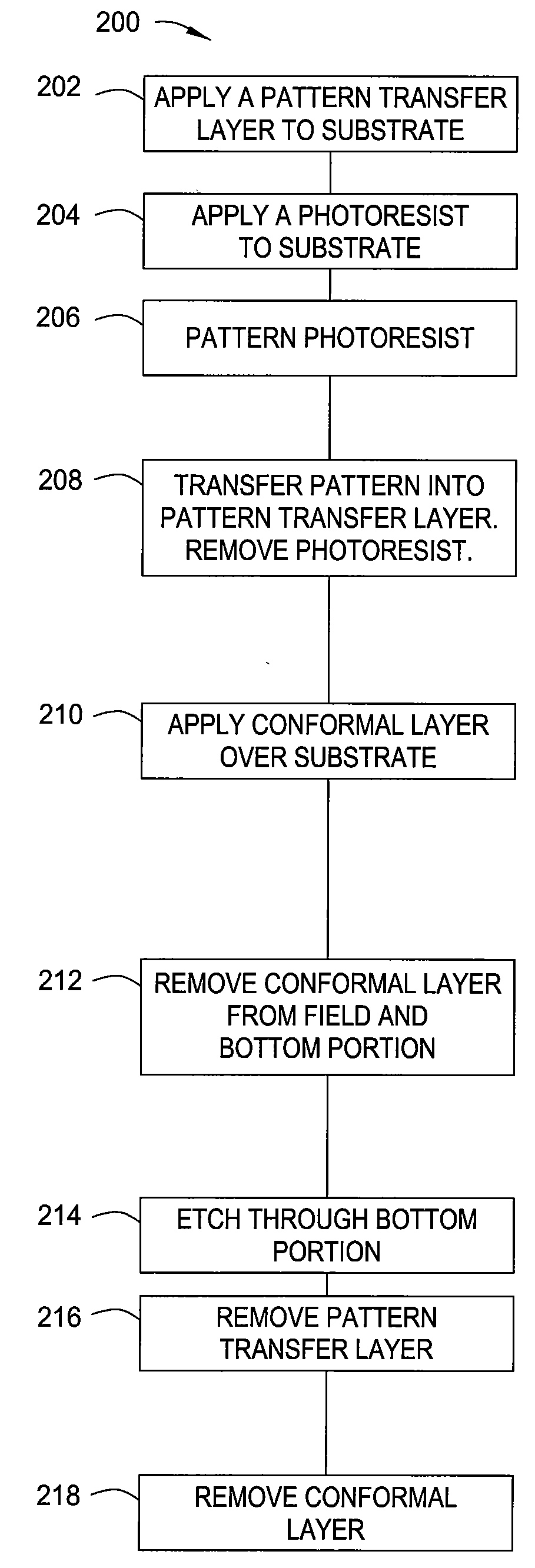
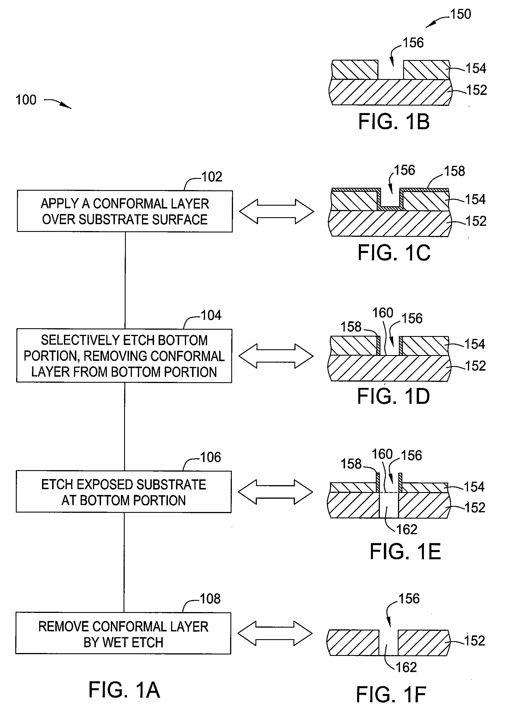
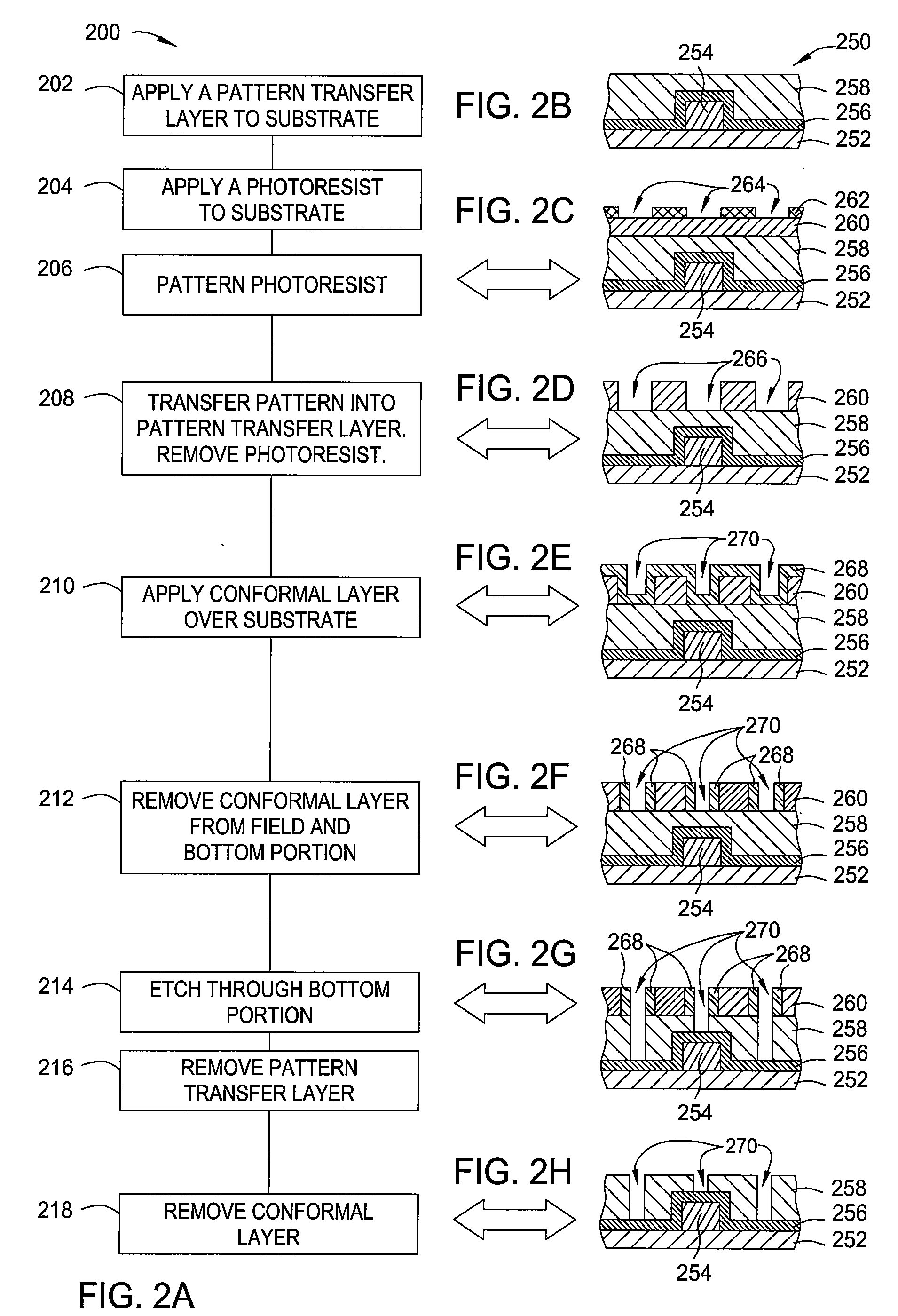
[0024]FIG. 1A is a flow diagram describing a method 100 according to one embodiment of the invention. FIGS. 1B-1F are schematic views of a substrate 150 at various stages of the method 100. A substrate such as the substrate 150 having a recess formed therein is provided to a processing chamber. FIG. 1B illustrates the substrate 150 with a feature layer 152 that is to be etched and a recess or opening 156 formed in a pattern transfer layer 154 overlying the feature layer 152. The feature layer 152 may be a dielectric or semiconductor layer of any sort desirous of etching. Pattern transfer layer 154 may be a hard mask layer, an anti-reflective layer, a dielectric layer, or any combination thereof....
PUM
 Abstract
Description
Claims
Application Information