Electronic device and method of manufacturing the same

a technology of electronic devices and manufacturing methods, applied in the field of electronic devices, can solve the problems of difficulty in small-scale development, deformation of adhesiveness between the hollow ceramic cap b>8/b> and the resin layer b>11/b>, and inability to maintain air tightness, etc., to achieve the effect of simple procedure, reduced cost and improved yield ratio

Inactive Publication Date: 2009-11-26
RENESAS ELECTRONICS CORP
View PDF1 Cites 24 Cited by
  • Summary
  • Abstract
  • Description
  • Claims
  • Application Information

AI Technical Summary

Benefits of technology

[0031]According to the present invention, since the electronic component may be hollow-sealed by bonding the resin cap composed of two or more resin layers with the electro-conductive pattern, while placing the adhesive layer in between, so that an electronic device having the electronic component tightly hollow-sealed therein may be obtained by a simple procedure.
[0032]According to the electronic device

Problems solved by technology

In particular for those used in the microwave region at frequencies of 20 GHz or higher, it is extremely difficult to develop small-sized, low-price packages excellent in the electrical performances and air-tightness.
Another problem arose in that the adhesiveness between the hollow ceramic cap 8 and the resin layer 11 could occasionally be degraded, due to difference in the coefficient of thermal shrinkage of the hollow ceramic cap 8 and the resin layer 11.
As a consequence, the hollow ceramic cap 8 could not maintain the air-tightness inside thereof, and the situation occasionally resulted in intrusion of moisture into the ceramic cap 8, or intrusion of solder flux or the like in the process of mounting th

Method used


Image

  • Electronic device and method of manufacturing the same
  • Electronic device and method of manufacturing the same
  • Electronic device and method of manufacturing the same

Examples


first embodiment

[0043]This embodiment will be explained referring to an exemplary case where a semiconductor device was formed as the electronic device.

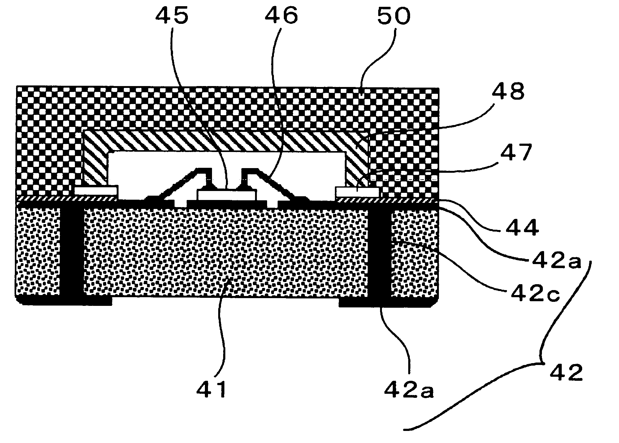
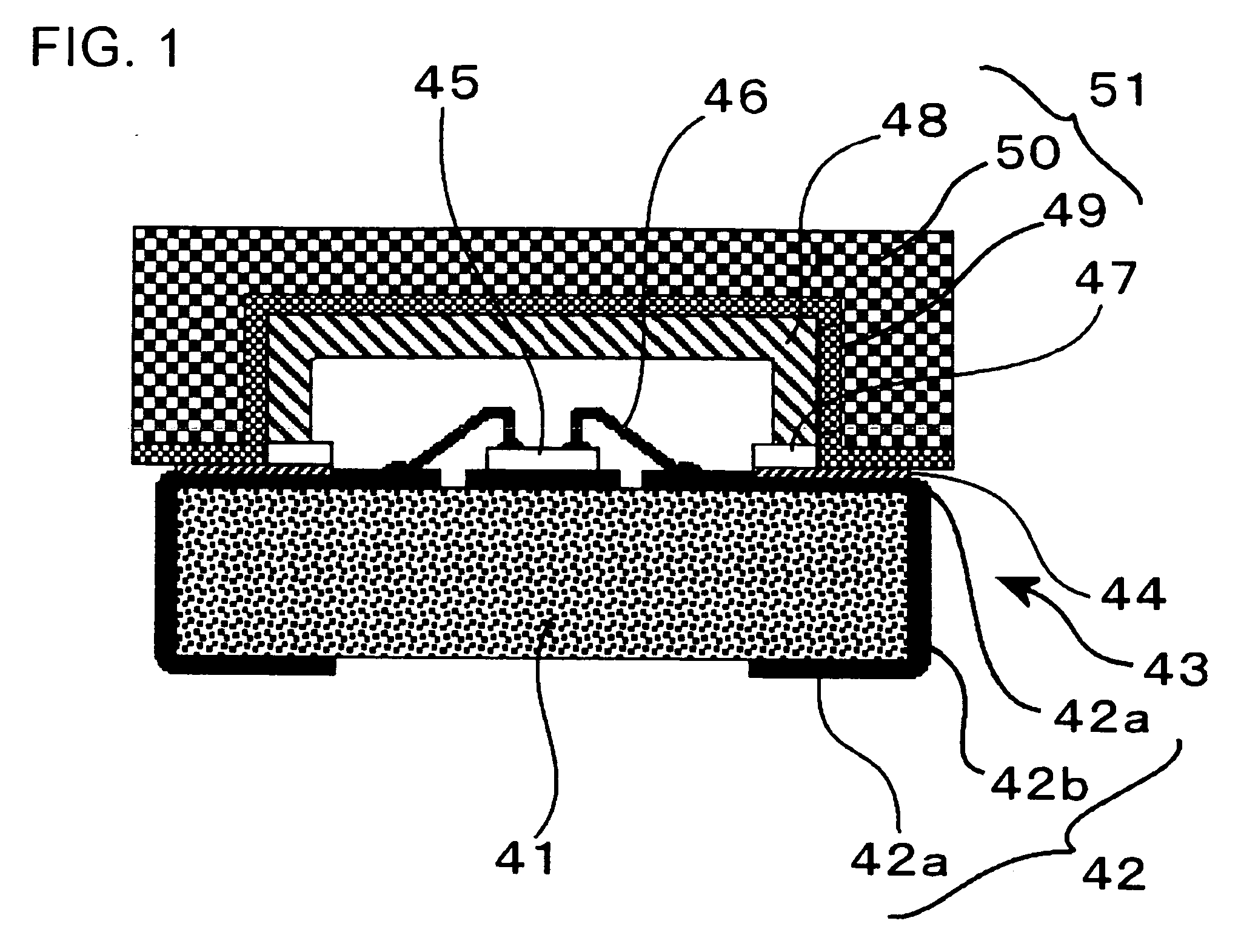
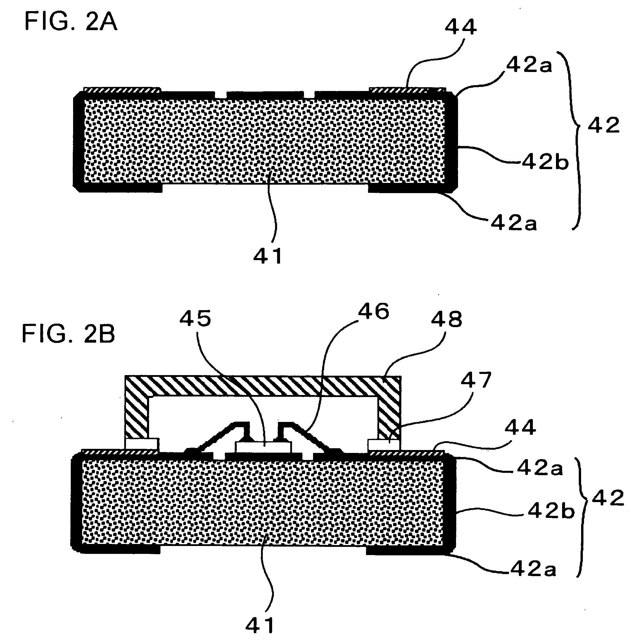
[0044]The semiconductor device of this embodiment has, as illustrated in FIG. 1, a substrate 41, an electro-conductive pattern (electrodes 42) provided over the substrate 41, an electronic component (semiconductor chip 45) mounted over the substrate 41, and electrically connected with the electrodes 42, a resin cap 51 provided over the substrate 41 so as to hollow-seal the semiconductor chip 45, and composed of three resin layers (a first resin layer 48, a second resin layer 49, and a third resin layer 50), and the adhesive layer (metal-resin adhesion maintenance layer 44) bonding the resin cap 51 with the electrodes 42.

[0045]The substrate 41 adoptable to this embodiment has a plurality of through-holes (viaholes 43) as illustrated in FIG. 4. Dielectric materials such as alumina ceramics, low temperature co-fired ceramics (LTCC); resin material such...

second embodiment

[0098]Next, a configuration of an electronic device according to a second embodiment of the present invention will be explained, referring to FIG. 5.

[0099]The semiconductor device of this embodiment has the electrodes 42a, 42a exposed to both surfaces of the substrate 41, wherein the electrodes 42a, 42a are connected through the via-filling metallized layers 42c.

[0100]Accordingly, the resin used in the first embodiment for forming the third resin layer 50 may be prevented from creeping onto the back surface, so that the second resin layer 49 is no more necessary, and thereby the structure may be simplified. Therefore, the semiconductor device having a semiconductor chip reliably hollow-sealed therein may be obtained by a further simplified method.

[0101]The embodiments of the present invention have been described referring to the attached drawings, merely as exemplary cases of the present invention, while allowing adoption of various configurations other than those described in the ...


PUM

PropertyMeasurementUnit
Thicknessaaaaaaaaaa
Electrical conductoraaaaaaaaaa
Frequencyaaaaaaaaaa

Abstract

An electronic device of the present invention has a substrate; an electro-conductive pattern (electrodes) provided over the substrate; a semiconductor chip mounted over the substrate, and electrically connected with the electrodes; a resin cap provided over the substrate and composed of two or more resin layers to hollow-sealing the semiconductor chip; and an adhesive layer (metal-resin adhesion maintenance layer) bonding the resin cap with the electrode.

Description

[0001]This application is based on Japanese patent application No. 2008-131991 the content of which is incorporated hereinto by reference.BACKGROUND[0002]1. Technical Field[0003]The present invention relates to an electronic device configured to hollow-seal an electronic component, and a method of manufacturing the same.[0004]2. Related Art[0005]Recent demands on higher performance, higher quality, smaller size and lower price of electronic devices have raised essential needs of improvement and sophistication of not only the devices per se, but also packages surrounding the devices. In particular for those used in the microwave region at frequencies of 20 GHz or higher, it is extremely difficult to develop small-sized, low-price packages excellent in the electrical performances and air-tightness. The packages may, therefore, expand their applications if the performances and quality durable under applications in the microwave region may be achieved only with inexpensive resin materia...

Claims


Application Information

Patent Timeline
IPC IPC(8): H05K5/06B29C65/00B32B37/00B32B7/12
CPCH01L2924/01013Y10T156/1089H01L2924/01033H01L2924/01079H01L2924/01082H01L2924/09701H01L2924/10329H01L2924/16152H01L2924/16315H01L2924/166H01L2924/01027Y10T156/1052H01L2924/1306H01L2224/32225H01L2924/01055H01L2924/01006H01L2924/01005H01L2224/97H01L2224/73265H01L2224/48465H01L2224/48227H01L2224/48095H01L24/97H01L24/48H01L23/10H01L23/06H01L23/055H01L2924/00012H01L2924/00H01L2224/451H01L2924/15787H01L2924/00014H01L24/73H01L2224/45099H01L2224/05599
Inventor HIROKAWA, TOMOAKIMATSUNOSHITA, MAKOTOKAKUTA, YUJISAKURA, NAOKI
Owner RENESAS ELECTRONICS CORP
Why Eureka
Try Eureka