Organic photoelectric conversion material and organic thin-film photoelectric conversion device

a conversion device and organic technology, applied in the field of organic photoelectric conversion material and organic thin-film photoelectric conversion device, can solve the problems of insufficient photoelectric conversion performance of conventional organic photoelectric conversion device to that of silicon photoelectric conversion device, insufficient use of long wavelength range (near infrared range) and insufficient use of long wavelength range (near infrared range). to achieve good photoelectric conversion performan

Active Publication Date: 2009-12-03
FUJIFILM CORP
View PDF1 Cites 14 Cited by
  • Summary
  • Abstract
  • Description
  • Claims
  • Application Information

AI Technical Summary

Benefits of technology

[0011]According to the present invention, it is possible to obtain an organic photoelectric conversion material capable of forming a film by using a coating method, and capable of providing a good photoelectric conversion performance even in a long wavelength range (near infrared range). Further, a high-performance organic thin-film photoelectric conversion device with sensitivity in the near infrared range may be obtained by using the organic photoelectric conversion material.

Problems solved by technology

For such a terminal, flexible, light-weight, and inexpensive electronic devices are required, but the conventional devices using inorganic semiconductor materials such as silicon does not sufficiently meet the requirement.
However, the photoelectric conversion performance of the conventional organic photoelectric conversion device is inferior to that of a silicon photoelectric conversion device.
The most outstanding issue to improvement in performance is that especially a long wavelength range (near infrared range) has not been used in the current device using both P3HT and PCBM because of a narrow light absorption wavelength range of the materials that are used in the device.
Resultantly, energy conversion efficiency is low for use of the solar cell, and sensitivity that is required for an optical sensor is not provided in the long wavelength range (near infrared range).
However, there is no specific description in which the croconium dye is actually used in an organic photoelectric conversion device.
Consequently, no photoelectric conversion performance is confirmed.

Method used


Image

  • Organic photoelectric conversion material and organic thin-film photoelectric conversion device
  • Organic photoelectric conversion material and organic thin-film photoelectric conversion device
  • Organic photoelectric conversion material and organic thin-film photoelectric conversion device

Examples


example 1

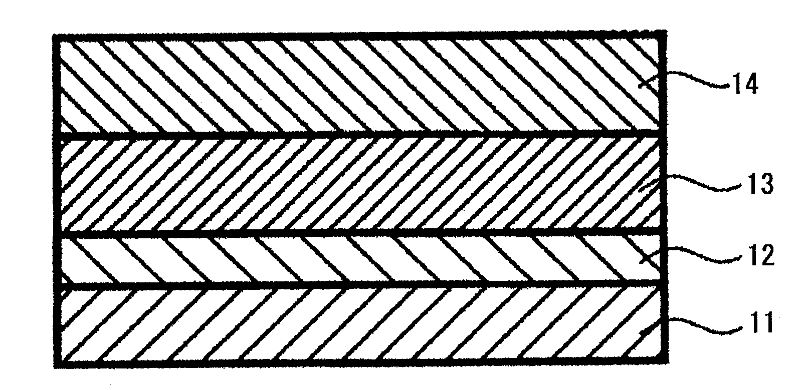
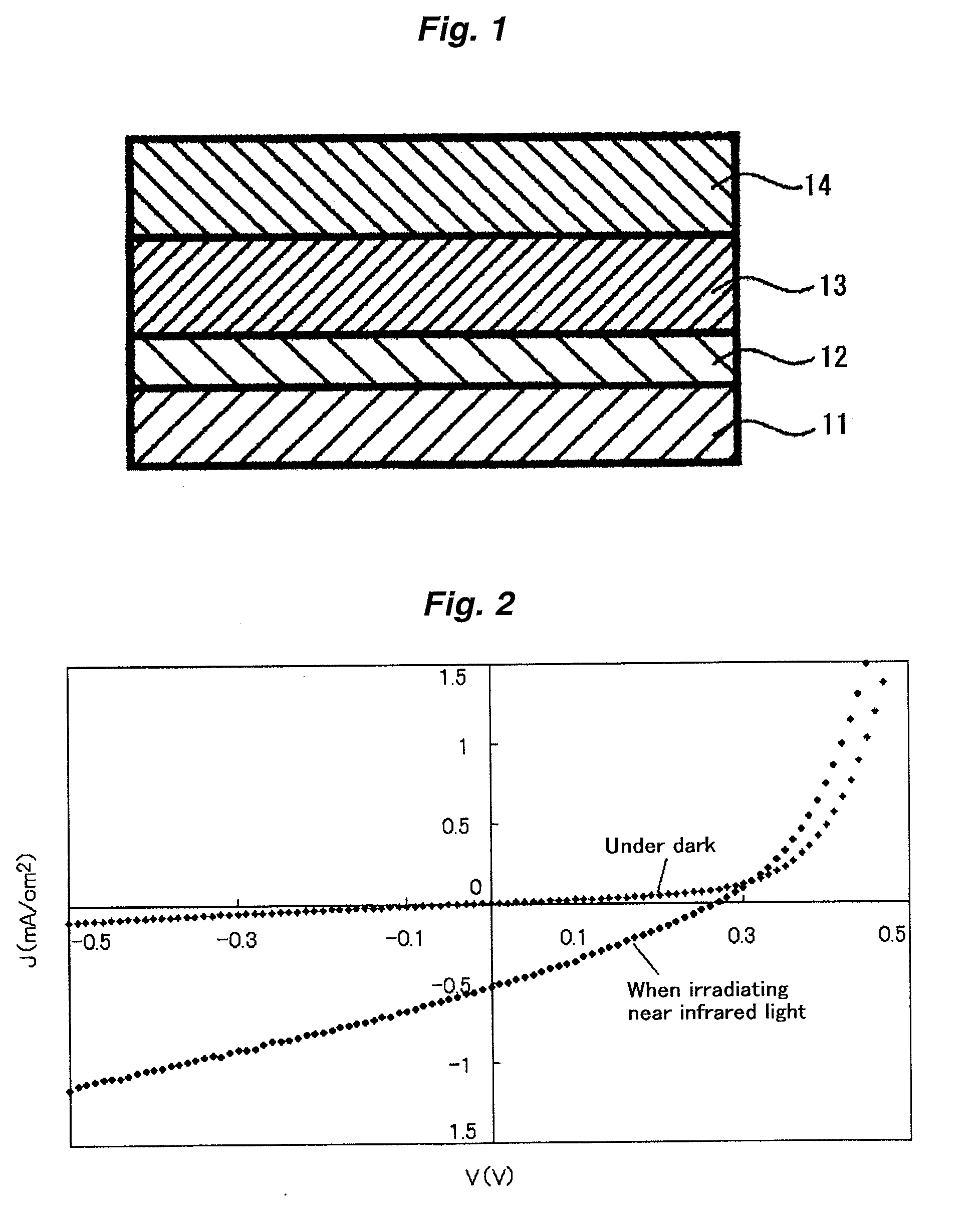
[0052]A glass substrate (2.5 cm×2.5 cm) with a patterning of ITO electrode was washed in isopropyl alcohol using ultrasonic, and then dried. Thereafter, a UV ozone treatment was performed for 30 minutes in order to remove organic contaminants on the surface of ITO substrate. Subsequently, an aqueous solution containing PEDOT (poly (3,4-ethylenedioxythiophene)) / PSS (polystyrene sulfonic acid) (Baytron P standard good) was spin coated on the ITO substrate at 4000 rpm for 60 seconds, and then dried at 120° C. for 10 minutes. Thereby, a 50 nm film-thick buffer layer was formed. The film thickness was measured using a film thickness meter by a stylus method (DEKTAK6M (trade name) manufactured by ULVAC, Inc.). Hereinafter, the same measuring method is applied to the film thickness. Subsequently, after dissolving 10 mg of the exemplified compound 1 and 10 mg of PCBM in 1 ml of 1,2-dichlorobenzene (HPLC grade) in a glove box (nitrogen atmosphere), ultrasonic was irradiated to the above mixt...

example 2

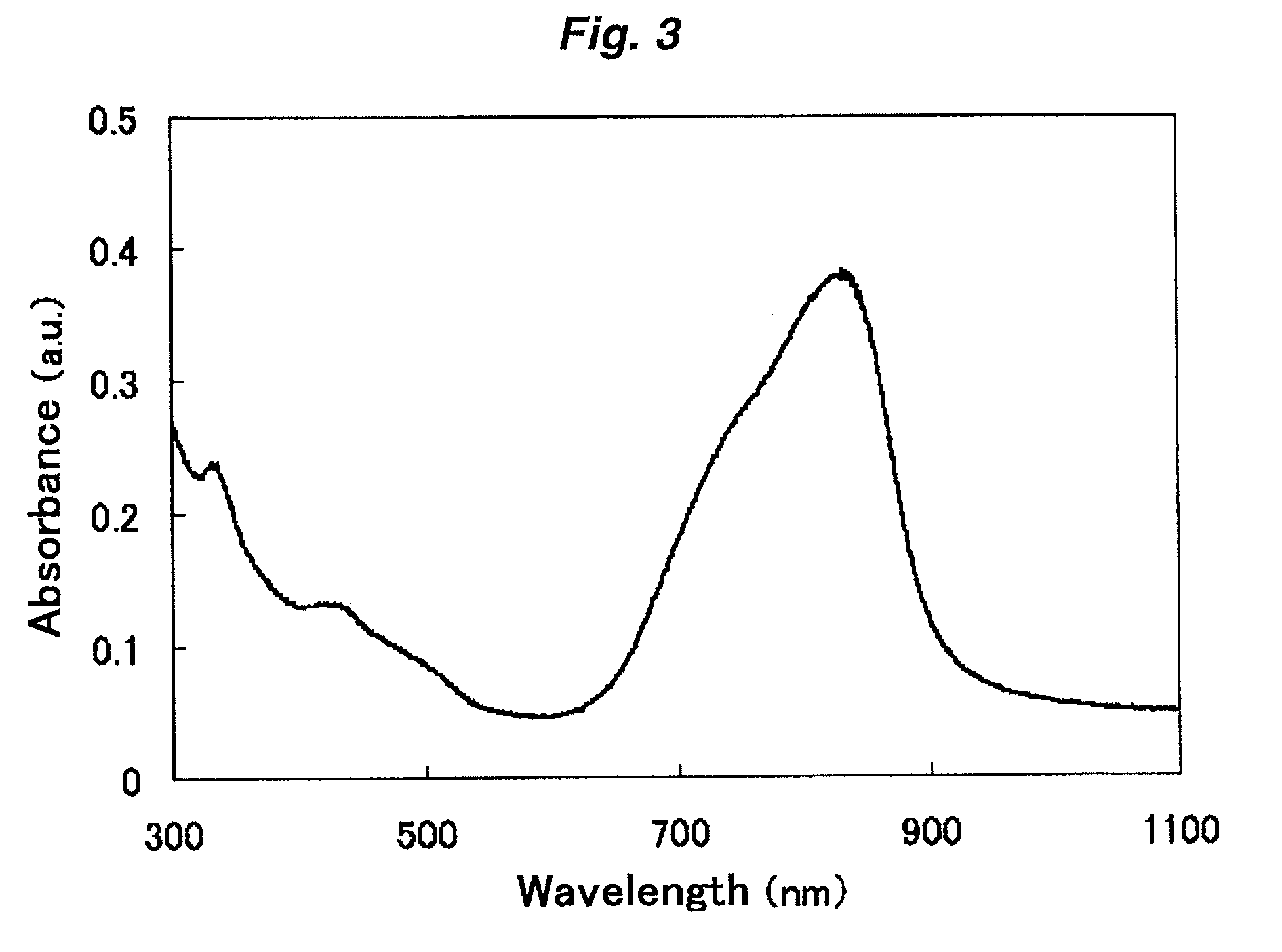
[0055]Devices manufactured exactly in the same manner as Example 1 except that each of the exemplified compounds 5, 9, 16, and 18 was used in place of the exemplified compound 1 respectively exhibited high photoelectric conversion performance equivalent to the device of Example 1 at the near infrared range. The results of short circuit-current, open voltage, and absorption λ max of the photoelectric conversion layer of each of the devices are shown in Table 1.


PUM

PropertyMeasurementUnit
boiling pointaaaaaaaaaa
thicknessaaaaaaaaaa

Abstract

An organic photoelectric conversion material for use in an organic thin-film photoelectric conversion device, containing a compound represented by formula 1; and an organic thin-film photoelectric conversion device having a photoelectric conversion layer which containing the organic photoelectric conversion material:wherein D represents an electron-donating aromatic substituent whose bonding site atom is a sp2 carbon atom; and a plurality of D may be the same or different from each other.

Description

FIELD OF THE INVENTION[0001]The present invention relates to an organic photoelectric conversion material containing a compound having a particular chemical structure, and to a high-performance organic thin-film photoelectric conversion device using the organic photoelectric conversion material.BACKGROUND OF THE INVENTION[0002]With the arrival of a ubiquitous information society, an information terminal is demanded to transfer information anytime, anywhere. For such a terminal, flexible, light-weight, and inexpensive electronic devices are required, but the conventional devices using inorganic semiconductor materials such as silicon does not sufficiently meet the requirement. Accordingly, in recent years, electronic devices using organic semiconductor materials as semiconductors are intensively studied for satisfying such requirements (see, for example, Chemical Reviews, 2007, 107, p. 1296-1323, and “Organic Field-Effect Transistors”, 2007, CRC Press, p. 159-228).[0003]Organic semic...

Claims


Application Information

Patent Timeline
Patent Type & Authority Applications(United States)
IPC IPC(8): H01L31/00C07D209/04
CPCB82Y10/00C07D401/10C07D403/10C07D407/10C07D409/10C07D413/10H01L51/4253C07D471/04H01L51/0047H01L51/005H01L51/0059H01L51/0067H01L51/0068C07D417/10H10K85/215H10K85/60H10K85/655H10K85/631H10K85/654H10K30/30
Inventor KITAMURA, TETSU
Owner FUJIFILM CORP
Why Eureka
Try Eureka