

Electromagnetic field detecting element and device using same
a technology of electromagnetic field and detection element, applied in the direction of nanoinformatics, optical radiation measurement, instruments, etc., can solve the problem of difficult detection of recorded information, and achieve the effect of simple structure, high efficiency of electromagnetic field detection, and easy production of elements
- Summary
- Abstract
- Description
- Claims
- Application Information
AI Technical Summary
Benefits of technology
Problems solved by technology
Method used
Image

Examples
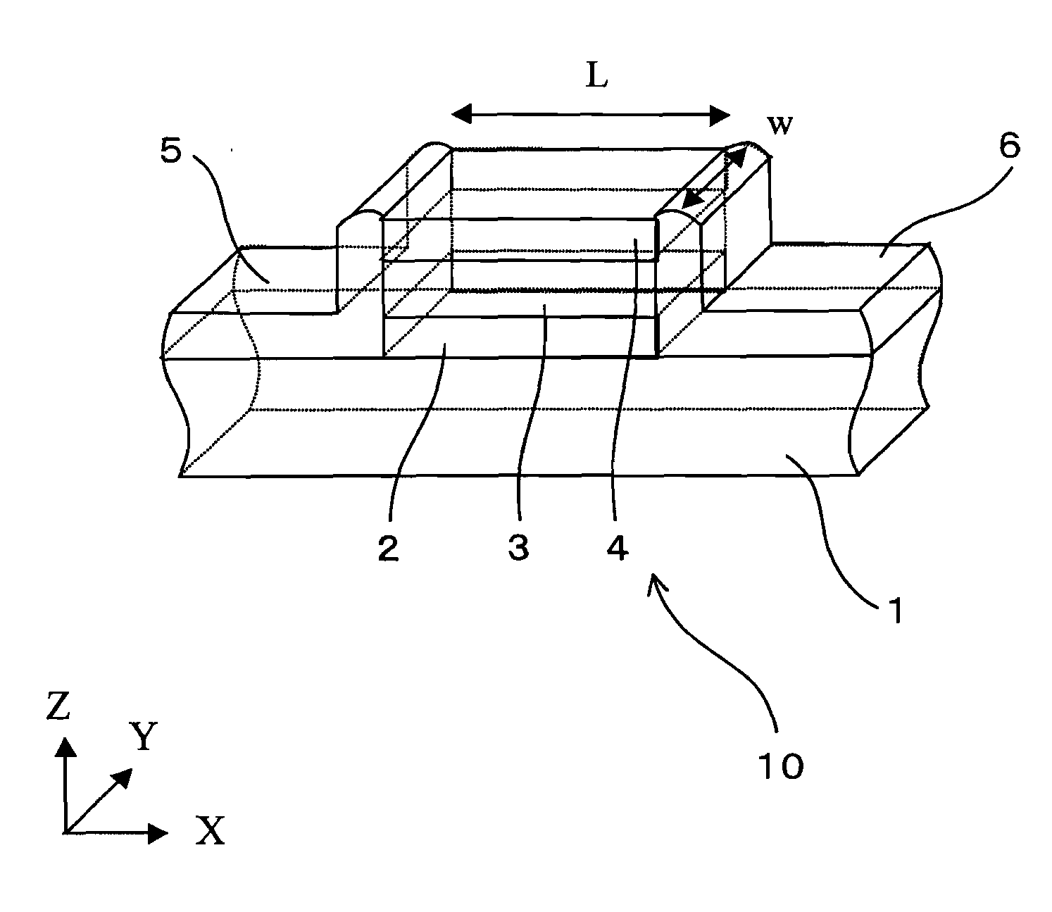
embodiment 1
Alternative Form 2 of Embodiment 1
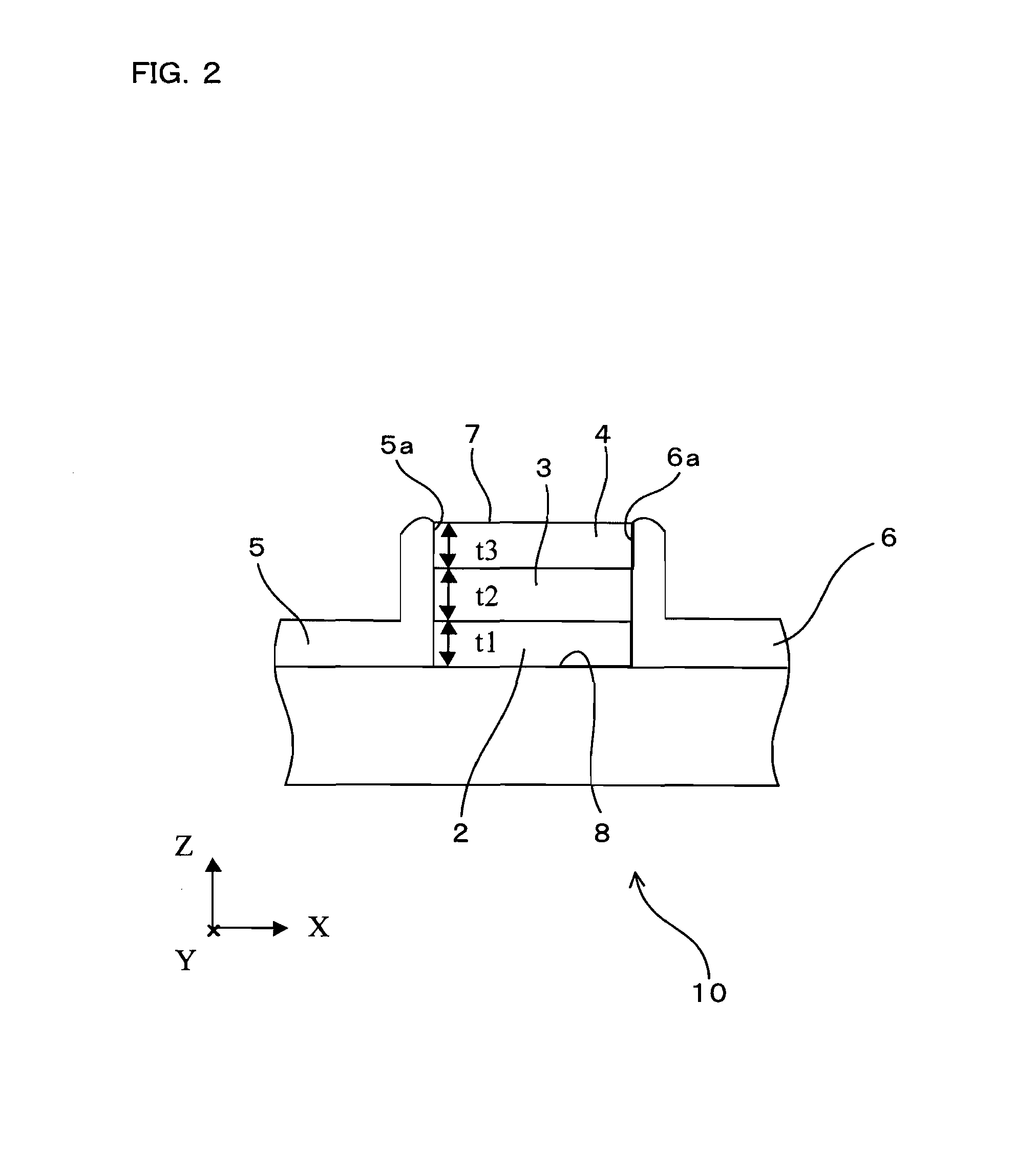
[0068]Next, the following describes Alternative Form 2 of Embodiment 1. The same symbols are given to parts that are identical to those described in Embodiment 1, and explanations therefor may be omitted below. FIG. 5 is a diagram showing the configuration of Alternative Form 2 of the electromagnetic field detecting element of Embodiment 1, viewed in a Y-axis direction. In the electromagnetic field detecting element 30, the insulation layer 33 has a length in a direction towards which the electrodes 35 and 36 face each other, which length differs from those of the insulation layers 32 and 34, and the insulation layers 32 and 34 are shorter than the insulation layer 33. In other words, an opposing surface of each of the electrodes 35 and 36 has a recessed portion. In the figure, reference symbols P1, Q1, P2, and Q2 are given to indicate corners of boundaries between the recessed portion and outside the recessed portion. Intervals P1-P2 and Q1-Q2 are ...
embodiment 2
[0070]Next, the following describes an electromagnetic field detecting circuit of Embodiment 2 according to the present invention. Members that are identical to those of Embodiment 1 are given symbols which are the same as those given to the members of Embodiment 1 except in that “4” is given in the tenth place. Explanation for those members may be omitted below.
[0071]FIG. 6 is a schematic diagram showing an electromagnetic field detecting circuit of Embodiment 2 in accordance with the present invention. FIG. 7 is a perspective configuration view specifically showing a relation between a magnetic field generating source and the electromagnetic field detecting element of the electromagnetic field detecting circuit of FIG. 6. As shown in FIG. 6, an electromagnetic field detecting circuit 100 of the present embodiment includes an electromagnetic field detecting sensor 101 and a phase controlling circuit 102.
[0072]The electromagnetic field detecting sensor 101 includes: an electromagnet...
embodiment 3
[0083]Next, the following describes an electromagnetic field detecting circuit of Embodiment 3, according to the present invention. Members that are identical to those of Embodiment 1 are given symbols which are the same as those given to the members of Embodiment 1 except in that “5” is given in the tenth place. Explanation for those members may be omitted below. Further, the parts of the present embodiment given the reference numerals 201, 202, 204 to 210, and 213 to 216 respectively correspond to the parts of Embodiment 2 with the reference numerals 101, 102, 104 to 110, and 113 to 116, and therefore explanations for these part may be omitted.
[0084]FIG. 8 is a schematic diagram showing an electromagnetic field detecting circuit of Embodiment 3 in accordance with the present invention. FIG. 9 is a perspective configuration view specifically showing a relation between an electric field generating source and the electromagnetic field detecting element of the electromagnetic field de...
PUM
| Property | Measurement | Unit |
|---|---|---|
| distance | aaaaa | aaaaa |
| dielectric constant | aaaaa | aaaaa |
| dielectric constant | aaaaa | aaaaa |
Abstract
Description
Claims
Application Information