Low index, large mode field diameter optical coupler

a technology of optical couplers and mode fields, applied in the field of optical couplers, can solve the problems of coupling loss, unstable laser, and auxiliary waveguide configuration, and achieve the effect of widening the bandwidth of optical signals

Active Publication Date: 2009-12-03
CISCO TECH INC
View PDF14 Cites 70 Cited by
  • Summary
  • Abstract
  • Description
  • Claims
  • Application Information

AI Technical Summary

Benefits of technology

[0017]It is an advantage of the arrangement of the present invention that the use of the larger-featured low index waveguide structure relaxes some of the stringent sub-micron alignment tolerances of the prior art, while maintaining efficient conversion between a first element supporting a large mode field optical signal and a second element supporting a small mode field optical signal. The relaxation of the alignment tolerances also allows for a wider bandwidth of optical signals to be utilized.

Problems solved by technology

However, the presence of the high index nanotaper tip at the junction where the incoming signal couples into the optical substrate has been found to generate back-reflections, presenting problems when attempting to directly couple light from a laser facet into the waveguide.
In fact, the back-reflections may cause the laser to become unstable.
Even when using such an auxiliary waveguide, coupling loss occurs as a result of mis-alignment between the incoming optical signal and the auxiliary waveguide.
The configuration of the auxiliary waveguide also contributes to signal loss, associated with the incomplete mode conversion between the auxiliary waveguide and the nanotaper.

Method used


Image

  • Low index, large mode field diameter optical coupler
  • Low index, large mode field diameter optical coupler
  • Low index, large mode field diameter optical coupler

Examples


Embodiment Construction

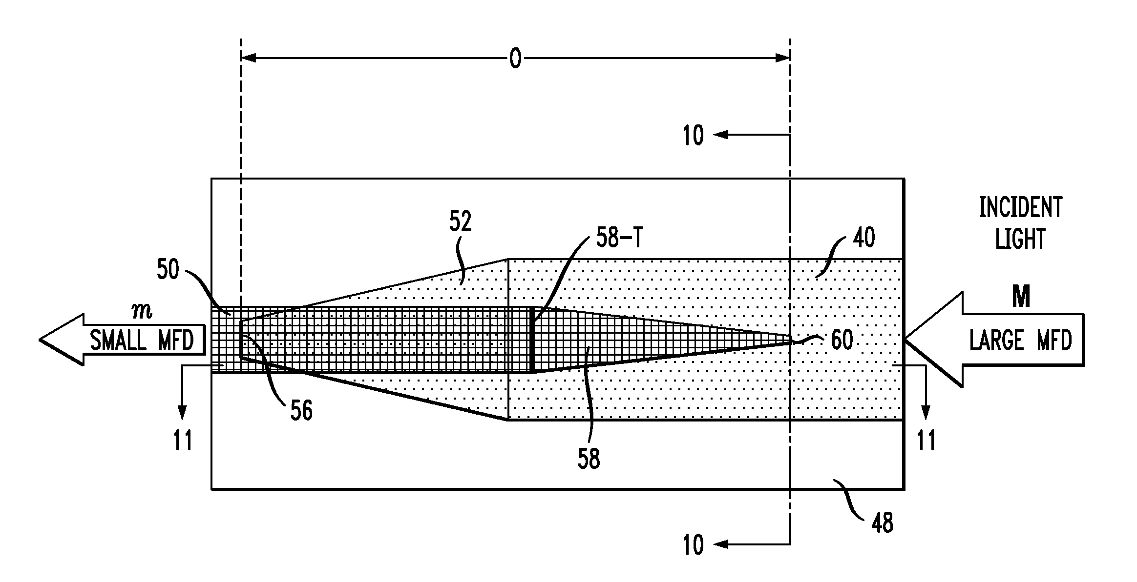
[0040]Free space optical signals, as well as signals from a light source or fiber, generally exhibit a large mode field diameter (when compared with, for example, the mode field supported by a single mode waveguide formed on a silicon-based optical substrate), requiring some type of mode conversion to provide efficient coupling into an optical waveguide with as little signal loss as possible. The utilization of a low index waveguide coupler, configured as described hereinbelow, is considered to provide improved coupling when compared to, for example, a prior art nanotaper coupler.

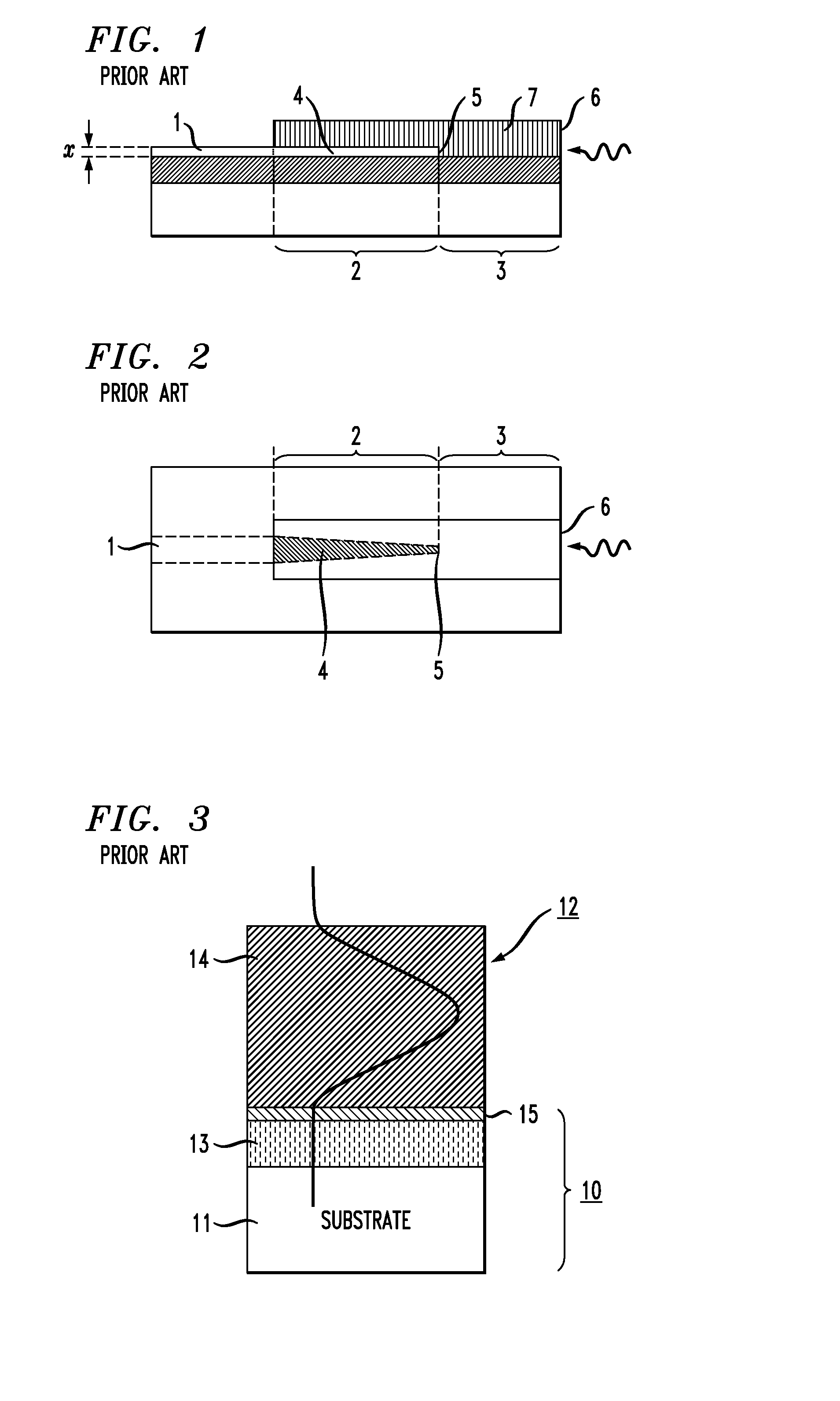
[0041]One type of low index waveguide that is suitable for use in the inventive coupler described below is an antiresonant reflecting optical waveguide (ARROW). Advantageously, an ARROW structure can be formed of the same materials that are used to form conventional silicon-based opto-electronic devices. FIG. 3 is a side view of an exemplary prior art arrangement of a silicon optical structure 10 and an ARR...


PUM


Abstract

An optical coupler is formed of a low index material and exhibits a mode field diameter suitable to provide efficient coupling between a free space optical signal (of large mode field diameter) and a single mode high index waveguide formed on an optical substrate. One embodiment comprises an antiresonant reflecting optical waveguide (ARROW) structure in conjunction with an embedded (high index) nanotaper coupling waveguide. Another embodiment utilizes a low index waveguide structure disposed in an overlapped arrangement with a high index nanotaper coupling waveguide. The low index waveguide itself includes a tapered region that overlies the nanotaper coupling waveguide to facilitate the transfer of the optical energy from the low index waveguide into an associated single mode high index waveguide. Methods of forming these devices using CMOS processes are also disclosed.

Description

CROSS-REFERENCE TO RELATED APPLICATIONS[0001]This application claims the benefit of the following provisional applications: U.S. Provisional Application 61 / 130,092, filed May 28, 2008; U.S. Provisional Application 61 / 131,106, filed Jun. 5, 2008; and U.S. Provisional Application 61 / 133,683, filed Jul. 1, 2008, all of which are herein incorporated by reference.TECHNICAL FIELD[0002]The present invention relates to an optical coupler and, more particularly, to an optical coupler formed of a low index material and exhibiting a mode field diameter suitable to provide efficient coupling between a free space optical signal (of large mode field diameter) and a waveguide of high index material formed on an optical substrate, the inventive coupler capable of operating over a relatively wide bandwidth.BACKGROUND OF THE INVENTION[0003]Advances in the art of coupling between an external optical signal and an optical waveguide have recently been associated with the use of an optical “nanotaper” st...

Claims


Application Information

Patent Timeline
Patent Type & Authority Applications(United States)
IPC IPC(8): G02B6/12G02B6/26
CPCG02B6/1228
Inventor WEBSTER, MARKPATEL, VIPULKUMAR
Owner CISCO TECH INC
Why Eureka
Try Eureka