Method and apparatus for chemical mechanical polishing of large size wafer with capability of polishing individual die

a technology of chemical mechanical polishing and individual dies, which is applied in the direction of grinding machine components, manufacturing tools, lapping machines, etc., can solve the problems of increasing the cost and complexity of a full wafer or production polisher, increasing the number of scale up problems, and increasing the difficulty of removing or significantly reducing the tool down time. , to achieve the effect of reducing the down time of tools, eliminating or significantly reducing the down tim

Inactive Publication Date: 2009-12-03
ST LAWRENCE NANOTECH
View PDF0 Cites 26 Cited by
  • Summary
  • Abstract
  • Description
  • Claims
  • Application Information

AI Technical Summary

Benefits of technology

[0009]The third aspect of the present invention is an effective and efficient method to achieve planarization on the selected area on the wafer surface or the entire wafer.
[0010]In an embodiment of the present invention as shown in FIG. 1, the wafer is hold on the platen, which is fixed and located below the multiple arms with polish heads, whereas the pads are attached to these polishing heads. The pad selection is mainly based on the film to be polished (copper, dielectric, barrier, metal, etc). There will be multiple sets of these polishing heads. Therefore, while one set is in operation of polishing, the other sets can be either conditioned or exchanged. This should eliminate or significantly reduce the tool down time. Whenever it is desired, the wafer can be covered by a specifically designed mask (FIG. 2) with the same number of windows as that of the dies on the wafer. These windows can be open, if the die located at the window will be polished; or closed so that the thin film is protected by the cover.

Problems solved by technology

Furthermore, on the 2″ wafers produced by this method only one die is usable.
Another motivation for adapting this approach is the ever increasing cost and complexity of a full wafer or production polisher.
It is widely recognized that, with the ever increase in wafer size, a number of scale up issues are becoming more and more apparent.
Significant effort has been spent and complicated schemes must be in place to maintain the within-wafer-non-uniformity for wafers larger than 200 mm.
It is increasingly difficult to optimize planarity at global level without severe over polishing at some local levels.
Furthermore, a compromise of such at lower level poses greater threat on defectivity at higher level.
In other words, with the significant increase in wafer size and challenges to maintain within wafer uniformity and defectivity, the conventional design is no longer a best choice.

Method used


Image

  • Method and apparatus for chemical mechanical polishing of large size wafer with capability of polishing individual die
  • Method and apparatus for chemical mechanical polishing of large size wafer with capability of polishing individual die
  • Method and apparatus for chemical mechanical polishing of large size wafer with capability of polishing individual die

Examples


Embodiment Construction

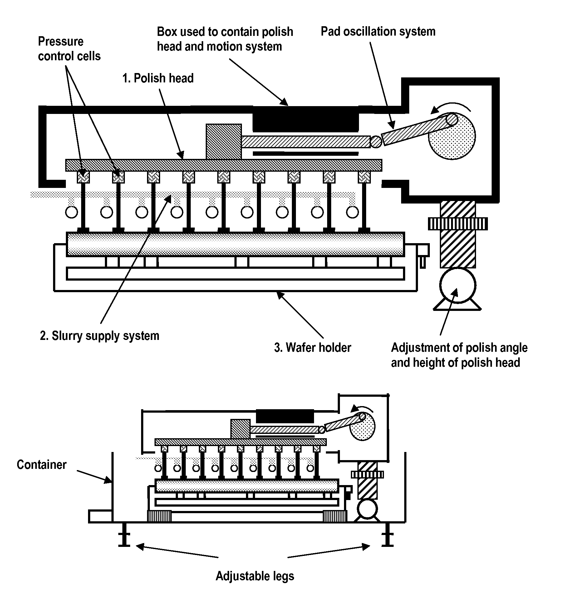
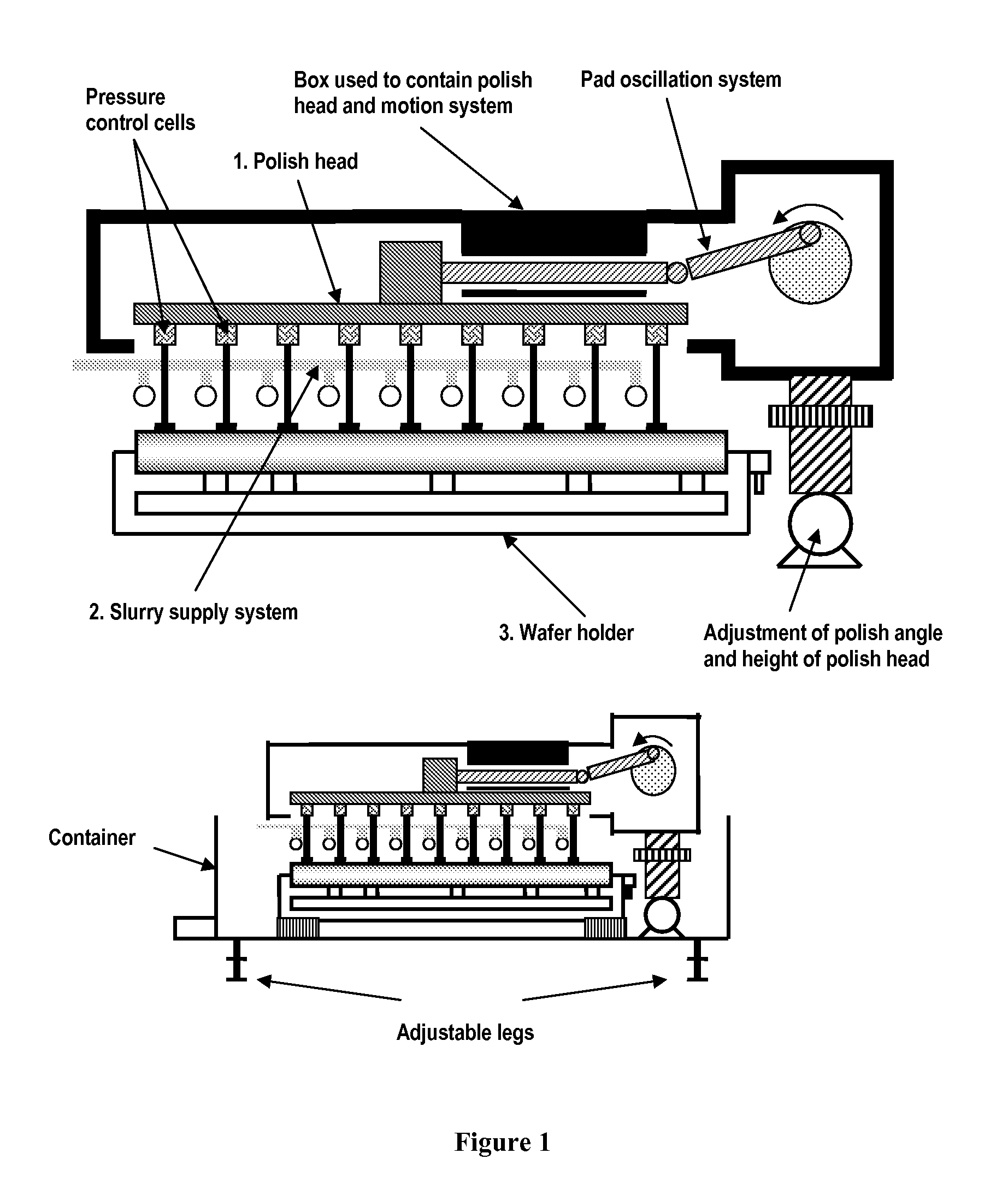
[0029]The present invention enables effective and efficient planarization of large wafer (12″, 18″,and beyond) with the capability of polishing individual die that need to be processed and easy control of within wafer uniformity, providing advantages over conventional CMP polisher. The present inventive design departs significantly from the traditional polisher design by focusing on each individual dies that need to be processed.

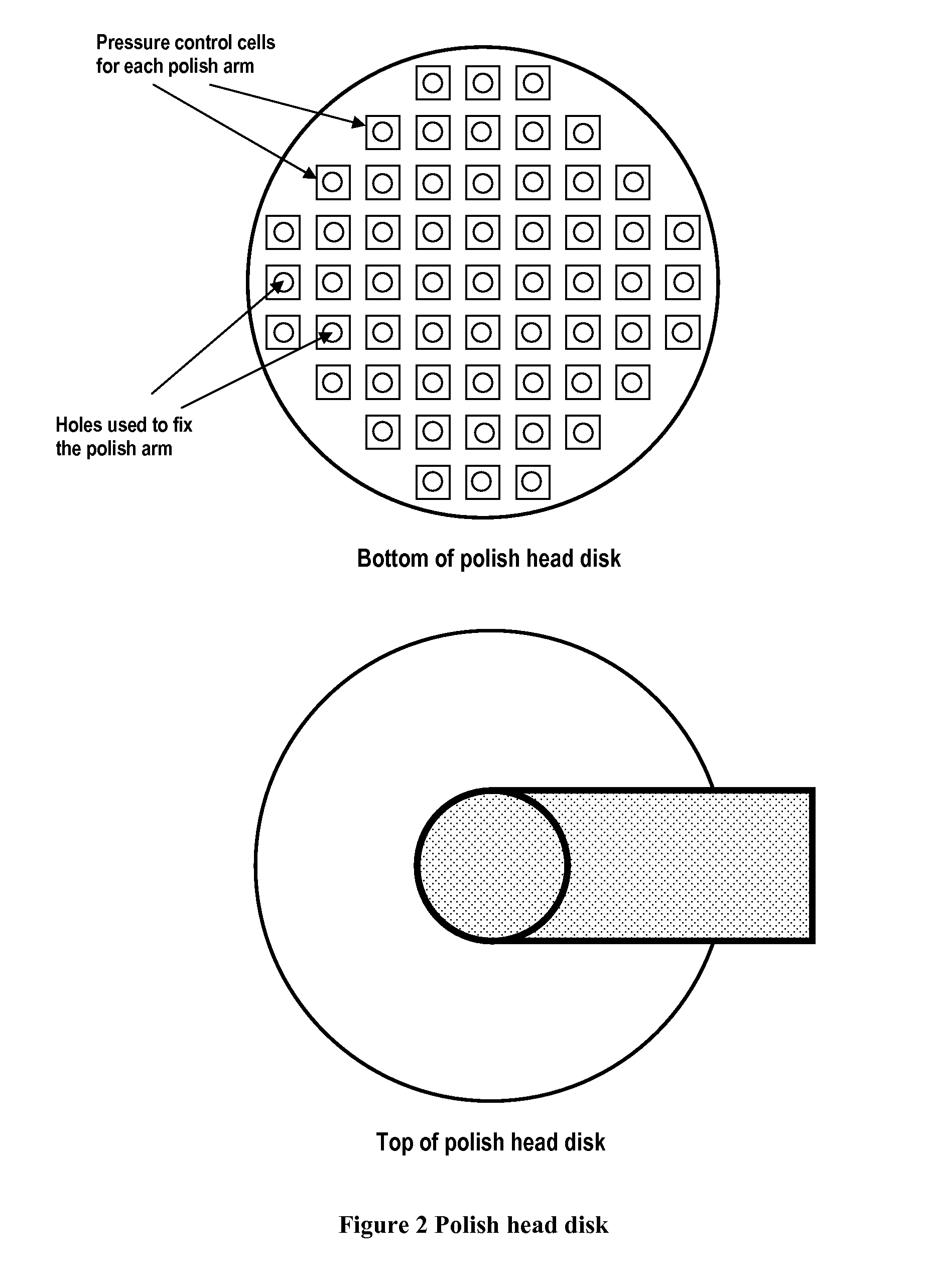
[0030]Aspects of the present invention are implemented by employing single polishing head with pad or multi-arms with polishing head to process one die or multiple dies on the wafer surface. In addition, the wafer is stationary. Conventional CMP polisher employs a large single pad, but only a portion of the pad is used as polish area. With this platform, it is difficult to process lager and lager wafers without the increase of pad size and the footprint of a polisher. The present invention overcomes this difficulty by switching the relative positions of the ...


PUM

PropertyMeasurementUnit
angleaaaaaaaaaa
radiusaaaaaaaaaa
diameteraaaaaaaaaa

Abstract

A novel polisher for chemical mechanical planarization process is described. The polisher design can have many variations. For process development and consumable evaluation, the CMP process can be performed on a single die or a section of the wafer. The size of testing wafer can be as small as 2″ and as large as 18″. Furthermore, several variations can characterize the slurry for their static etch rate, dynamic etch rate, material removal rate, and viscosity in a single experiment. For production level wafer processing, Chemical Mechanical Polishing of all dies on the wafer surface is achieved by using multi-armed polishing heads or a single polishing head with small piece of a pad at the bottom of the head. The within wafer uniformity can be easily controlled and the equipment can be easily scaled up or down. This inventive design may translate to significant cost reduction for wafer processing at production level as well as evaluation of consumables at research and development level.

Description

INCORPORATION BY REFERENCE[0001]Any foregoing applications and all documents cited therein or during their prosecution (“application cited documents”) and all documents cited or referenced in the application cited documents, and all documents cited or referenced herein (“herein cited documents”), and all documents cited or referenced in herein cited documents, together with any manufacturer's instructions, descriptions, product specifications, and product sheets for any products mentioned herein or in any document incorporated by reference herein, are hereby incorporated herein by reference, and may be employed in the practice of the invention.FIELD OF THE INVENTION[0002]This invention relates to a method of chemical mechanical polishing (CMP) for microelectronics applications. Specifically, the invention is directed to an apparatus of chemical mechanical polishing used for large size patterned / blanket wafer polishing, a process allowing polishing an individual die at a time, and a ...

Claims


Application Information

Patent Timeline
Patent Type & Authority Applications(United States)
IPC IPC(8): B24B1/04B24B7/22B24B49/10B24B49/12B24B37/04
CPCB24B21/04B24B37/04B24B57/02B24B37/30B24B49/10B24B37/105C23F1/02H01L21/302H01L21/304
Inventor LI, YUZHOUQIN, QINGJUNBURKHART, CRAIG
Owner ST LAWRENCE NANOTECH
Why Eureka
Try Eureka