Substrate Processing Apparatus and Substrate Processing Method

a substrate processing and substrate technology, applied in the direction of carpet cleaners, cleaning using liquids, lapping machines, etc., can solve the problems of large overall size and considerable time taken to transport substrates to components, and achieve the effect of preventing dust from adhering

Active Publication Date: 2009-12-10
EBARA CORP
View PDF4 Cites 20 Cited by
  • Summary
  • Abstract
  • Description
  • Claims
  • Application Information

AI Technical Summary

Benefits of technology

[0037]The substrate processing apparatus according to the present invention includes at least one of the ultrasonic cleaning device that cleans the surface of the substrate with ultrasonic waves transmitted through the liquid, and the two-fluid jet cleaning device that mixes gas and liquid together and spouts them as the two-fluid jet for cleaning the surface of the substrate. As a result, minute particles are removed with the fluid, and the substrate processing apparatus is made capable of cleaning the substrate without taking an initializing time while preventing dust from adhering to the substrate.
[0038]The substrate processing method according to the present invention includes the solid matter noncontact cleaning step of cleaning the surface of the substrate while bringing fluid into contact with the surface of the substrate, minute particles are removed with the fluid, making it possible to clean the surface of the substrate without taking an initializing time and without causing dust adhering to the substrate.

Problems solved by technology

Since polishing apparatuses include many components, they tend to be large in overall size.
Therefore, considerable amount of time has been taken to transport substrates to the components suitable for carrying out various steps.

Method used


Image

  • Substrate Processing Apparatus and Substrate Processing Method
  • Substrate Processing Apparatus and Substrate Processing Method
  • Substrate Processing Apparatus and Substrate Processing Method

Examples


example 1

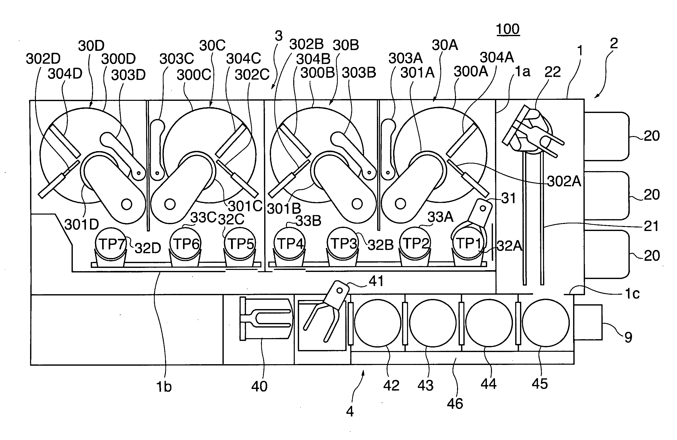
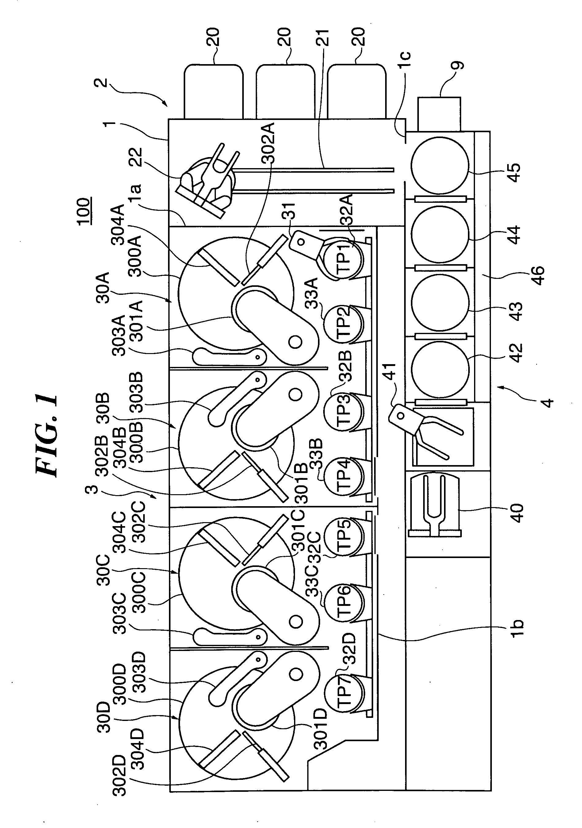
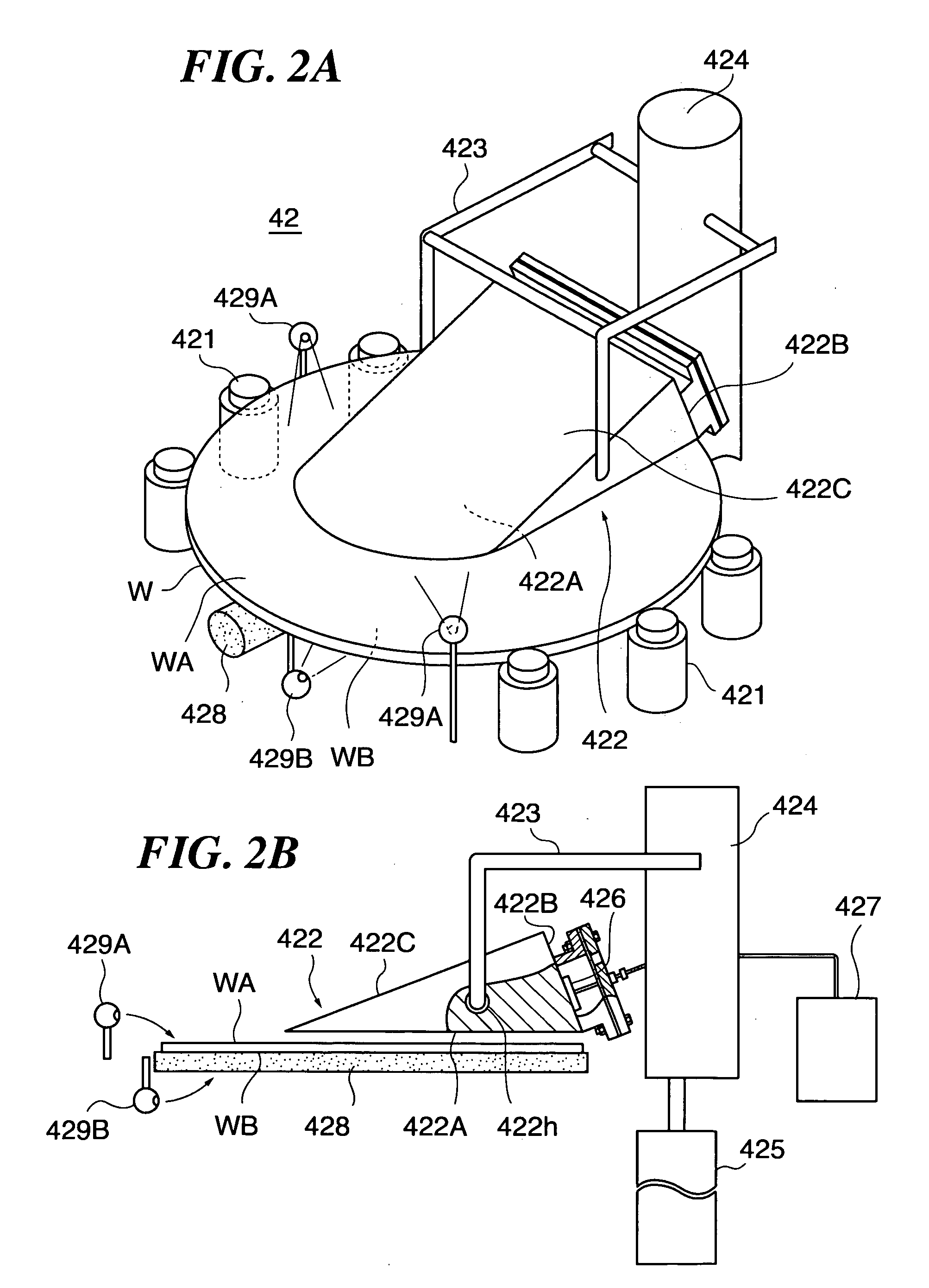
[0129]In the Example 1, the cleaning section 4 of the substrate processing apparatus 100 (See FIG. 1) was constituted by disposing components in the order of: the ultrasonic cleaner 42 (See FIG. 2), the roll cleaner 43 (See FIG. 4), the first two-fluid jet cleaner 44 (See FIG. 5), and the second two-fluid jet cleaner 44 (See FIG. 5), from the upstream to downstream side. The substrate W to be processed in the Example 1 was one with its top surface WA having grooves formed according to wiring pattern, a silicon dioxide (SiO2) film, and a titanium nitride (TiN) film as barrier metal; over which a tungsten film was formed. This substrate W was polished by a predetermined depth in the polishing section 3, so that SiO2, TiN, and tungsten appeared on the top surface WA of the substrate W. The top surface WA of the substrate W was adapted to have an alignment mark, remaining after being polished, used for example for positioning in manufacturing semiconductor devices; with the alignment ma...

example 2

[0138]In the Example 2, the cleaning section 4 of the substrate processing apparatus 100 (See FIG. 1) was constituted by disposing components in the order of: the first ultrasonic cleaner 42 (See FIG. 2), the second ultrasonic cleaner 42 (See FIG. 2), the first two-fluid jet cleaner 44 (See FIG. 5), and the second two-fluid jet cleaner 44 (See FIG. 2) from the upstream to downstream side. The substrate W to be processed in the Example 2 was made the same as that used in the Example 1 (substrate with SiO2 film plus TiN film plus tungsten film). This substrate W was polished by a predetermined amount in the polishing section 3, so that SiO2, TiN, and tungsten appeared on the top surface WA of the substrate W. Here, the top surface WA of the substrate W was adapted like that in the Example 1 to have an alignment mark, remaining after being polished; with the alignment mark made up of two grooves, each about 0.5 micrometers wide, 0.5 micrometers deep, and 5 micrometers long, crossing ea...

example 3

[0143]In the Example 3, the cleaning section 4 of the substrate processing apparatus 100 (See FIG. 1) was constituted by disposing components in the order of: the first ultrasonic cleaner 42 (See FIG. 2), the second ultrasonic cleaner 42 (See FIG. 2), the first two-fluid jet cleaner 44 (See FIG. 5), and the second two-fluid jet cleaner 44 (See FIG. 5), from the upstream to downstream side. The substrate W to be processed in the Example 3 was one with its top surface WA having grooves formed according to the wiring pattern, an SiO2 film, and a tantalum nitride (TaN) film as barrier metal; over which a copper (Cu) film was formed. First, the Cu film on the substrate W was polished down to the highest level of the TaN film (excluding the TaN film in the grooves matching the wiring pattern) on the top surface WA of the substrate W. Next, the substrate W was moved to the polishing device 30B to polish by 10 nm the TaN film on the highest level of the top surface WA of the substrate W and...


PUM

PropertyMeasurementUnit
widthaaaaaaaaaa
widthaaaaaaaaaa
depthaaaaaaaaaa

Abstract

A substrate processing apparatus includes: a polishing device 30A for polishing the surface of a substrate; and at least one of an ultrasonic cleaning device 42 for cleaning the surface of the substrate with ultrasonic waves transmitted through a liquid, and a two-fluid jet cleaning device 44 for cleaning the surface of the substrate with a two-fluid jet spouted as a mixture of a gas and a liquid. A substrate processing method includes: a polishing step of polishing the surface of a substrate; and a solid matter noncontact cleaning step of cleaning the surface of the substrate by spraying a liquid to the surface of the substrate. The above apparatus and method make it possible to efficiently clean the surface of a substrate after it is polished.

Description

TECHNICAL FIELD[0001]This invention relates to a substrate processing apparatus and a substrate processing method, and specifically relates to such apparatus and method that make it possible to efficiently clean substrates after they are polished.BACKGROUND ART[0002]Improvements in manufacturing technology for semiconductor devices in recent years have been remarkable. As semiconductor devices are made with ever higher degree of integration, circuit wiring becomes finer and spacing between wires becomes narrower. Amid such circumstances, semiconductor substrates are required to be made flat. As a means for flattening semiconductor substrates, a polishing apparatus is known that carries out chemical mechanical polishing (CMP). Since polishing apparatuses include many components, they tend to be large in overall size. Therefore, considerable amount of time has been taken to transport substrates to the components suitable for carrying out various steps. Under such circumstances, attemp...

Claims


Application Information

Patent Timeline
Patent Type & Authority Applications(United States)
IPC IPC(8): C25F3/30B08B3/12
CPCB08B3/02B08B3/12B08B2203/0288B24B37/04H01L21/67219H01L21/02074H01L21/67028H01L21/67046H01L21/67051H01L21/02052H01L21/302H01L21/304
Inventor OIKAWA, FUMITOSHIKAJITA, SHINJI
Owner EBARA CORP
Why Eureka
Try Eureka