

Silicon carbide semiconductor substrate and method of manufacturing the same
a technology of silicon carbide and semiconductor substrate, which is applied in the direction of basic electric elements, electrical apparatus, semiconductor devices, etc., can solve problems such as unsuitability, and achieve the effect of improving conversion efficiency and reducing the dislocation density of the basal plan
- Summary
- Abstract
- Description
- Claims
- Application Information
AI Technical Summary
Benefits of technology
Problems solved by technology
Method used
Image

Examples
first embodiment
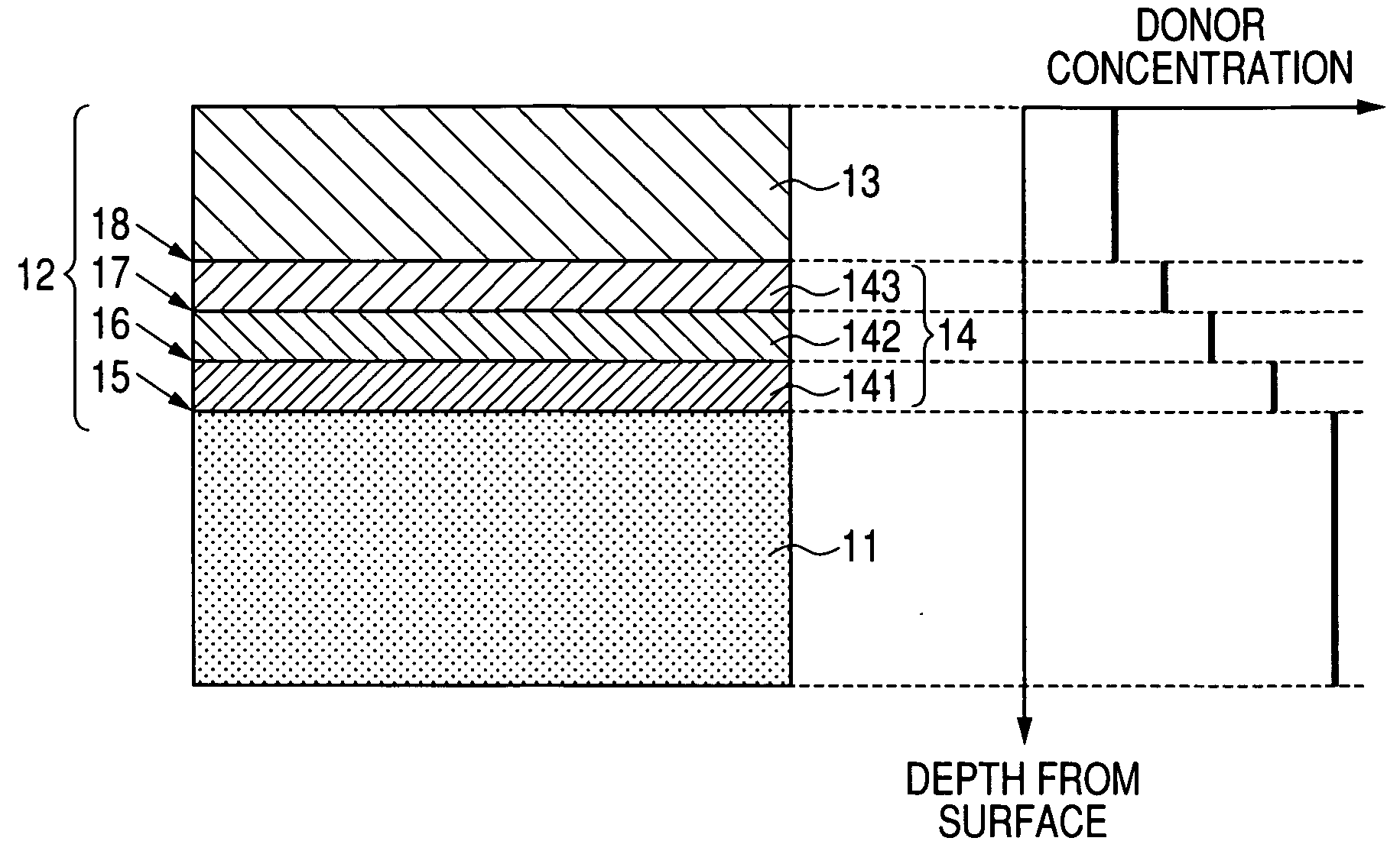
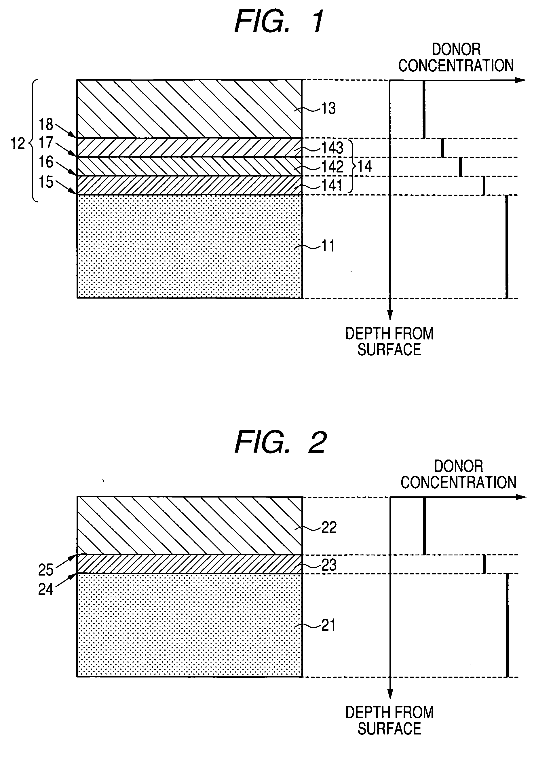
[0064]As a first embodiment of the present invention, a method of manufacturing a silicon carbide semiconductor substrate having a cross-sectional structure shown in FIG. 1 will be described.
[0065]FIGS. 5A to 5E are cross-sectional views showing a manufacturing process of a silicon carbide semiconductor substrate according to the first embodiment.
[0066]First, in the process shown in FIG. 5A, a base substrate 51 including a silicon carbide single crystal wafer is prepared. The silicon carbide single crystal wafer is an n-type 4H—SiC having a diameter of 50 mm and a (0001) Si plane inclined by 8° in a [11-20] direction, wherein donor concentration is 5×1018 cm−3. The silicon carbide single crystal wafer having a {0001} plane is a plane polarity, wherein one is a Si plane (described as a (0001) Si plane) whose outermost surface is made of silicon atoms and the other is a C plane (described as a (000-1) C plane) whose outermost surface is made of carbon atoms. The first embodiment uses ...
second embodiment
[0093]As a second embodiment of the present invention, a manufacturing method different from the first embodiment of the silicon carbide semiconductor substrate having the cross-sectional structure shown in FIG. 1 will be described.
[0094]FIGS. 8A to 8E are cross-sectional views showing a lo manufacturing process of a silicon carbide semiconductor substrate according to the second embodiment.
[0095]First, in the process shown in FIG. 8A, a base substrate 81 including the silicon carbide single crystal wafer is prepared. The silicon carbide single crystal wafer is the n-type 4H—SiC having a diameter of 50 mm and a (0001) Si plane inclined by 8° in a [11-20] direction, wherein the donor concentration is 5×1018 cm−3. The surface of the Si plane side of the wafer is subjected to the mechanical mirror polishing and then the CMP process.
[0096]Next, in the process shown in FIG. 8B, the base substrate 81 of FIG. 8A is subjected to an RCA cleaning and then installed in a susceptor of a reactor...
third embodiment
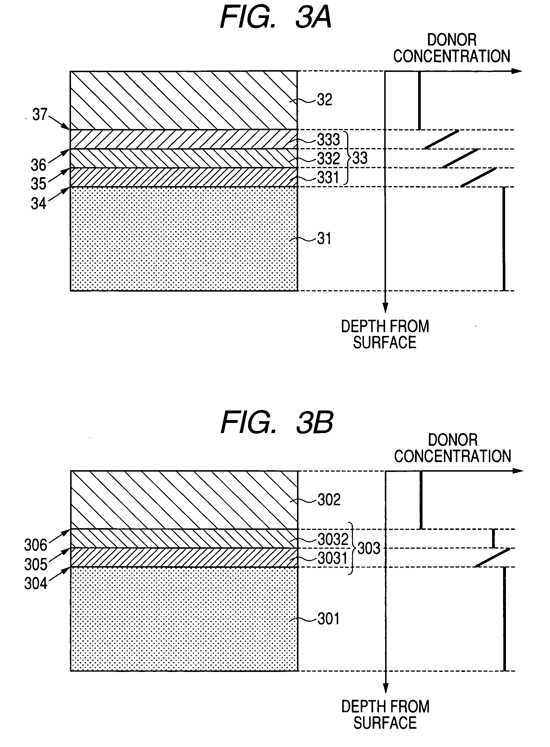
[0105]As a third embodiment of the present invention, a method of manufacturing a silicon carbide semiconductor substrate having a cross-sectional structure shown in FIG. 3A will be described.
[0106]FIGS. 9A to 9E are cross-sectional views showing a manufacturing process of a silicon carbide semiconductor substrate according to the third embodiment.
[0107]First, in the process shown in FIG. 9A, a base substrate 91 including the silicon carbide single crystal wafer is prepared. The silicon carbide single crystal wafer is the n-type 4H—SiC having a diameter of 50 mm and a (0001) Si plane inclined by 8° in a [11-20] direction, wherein the donor concentration is 5×1018 cm−3. The surface of the Si plane side of the wafer is subjected to the mechanical mirror polishing and then the CMP process. Next, in the process shown in FIG. 9B, the base substrate 91 of FIG. 9A is subjected to an RCA cleaning and then installed in a susceptor of a reactor in a hot-wall CVD system. Next, the reactor is d...
PUM
| Property | Measurement | Unit |
|---|---|---|
| temperature | aaaaa | aaaaa |
| covalent radius | aaaaa | aaaaa |
| covalent radius | aaaaa | aaaaa |
Abstract
Description
Claims
Application Information