Silicon carbide semiconductor substrate and silicon carbide semiconductor device by using thereof

a silicon carbide semiconductor and semiconductor substrate technology, applied in the direction of semiconductor devices, basic electric elements, electrical apparatus, etc., can solve the problems of inability to determine the donor concentration in the epitaxial layer adopted as the drift layer, the method is not suitable for forming an epitaxial layer, and the determination of the dislocation density cannot be achieved by mere reasoning only for reducing the dislocation density, etc., to achieve significant reduction enhancing conversion efficiency, and reducing the effect of basal plane dislocation density

Inactive Publication Date: 2009-04-02
HITACHI CABLE
View PDF3 Cites 53 Cited by
  • Summary
  • Abstract
  • Description
  • Claims
  • Application Information

AI Technical Summary

Benefits of technology

[0013]Methods for reducing the basal plane dislocation density in an epitaxial layer by enhancing the conversion efficiency at which the basal plane dislocations in the wafer are converted into threading edge dislocations include the method disclosed in, for example, JP-T-2007-506289. In the method of JP-T-2007-506289, a section with exposed basal plane dislocations on the surface of a silicon carbide single-crystal wafer is selectively etched to form a concave portion that primarily includes dislocations, and to thereby grow an epitaxial layer on the wafer. In the thus-formed epitaxial layer, as described in Materials Science Forum, Vols. 527-529, pp. 243-246, the basal plane dislocations are significantly reduced. However, as described in Materials Science Forum, Vols. 527-529, pp. 1329-1334, whereas the reliability of the on-state characteristics of a p-n junction built into such an epitaxial layer is surely improved by a decrease in basal plane dislocation density, the off-state characteristics of the p-n junction are conversely deteriorated by the decrease. This is probably because the growth of the epitaxial layer on the concave wafer has caused other crystal defects around the concave portion. The method in which the section on a silicon carbide single-crystal wafer surface where exposed basal plane dislocations exist is selectively etched to form a concave portion on the surface and grow an epitaxial layer on the wafer is effective for reducing the basal plane dislocation density. On the whole, however, this method is not suitable for forming an epitaxial layer into which to build a semiconductor device. What is needed is means for reducing the basal plane dislocation density in an epitaxial layer without affecting the film quality of the epitaxial layer in any forms.

Problems solved by technology

This is probably because the growth of the epitaxial layer on the concave wafer has caused other crystal defects around the concave portion.
On the whole, however, this method is not suitable for forming an epitaxial layer into which to build a semiconductor device.
The donor concentration in the epitaxial layer adopted as the drift layer, however, cannot be determined by mere reasoning only for reducing the dislocation density.

Method used


Image

  • Silicon carbide semiconductor substrate and silicon carbide semiconductor device by using thereof
  • Silicon carbide semiconductor substrate and silicon carbide semiconductor device by using thereof
  • Silicon carbide semiconductor substrate and silicon carbide semiconductor device by using thereof

Examples


first embodiment

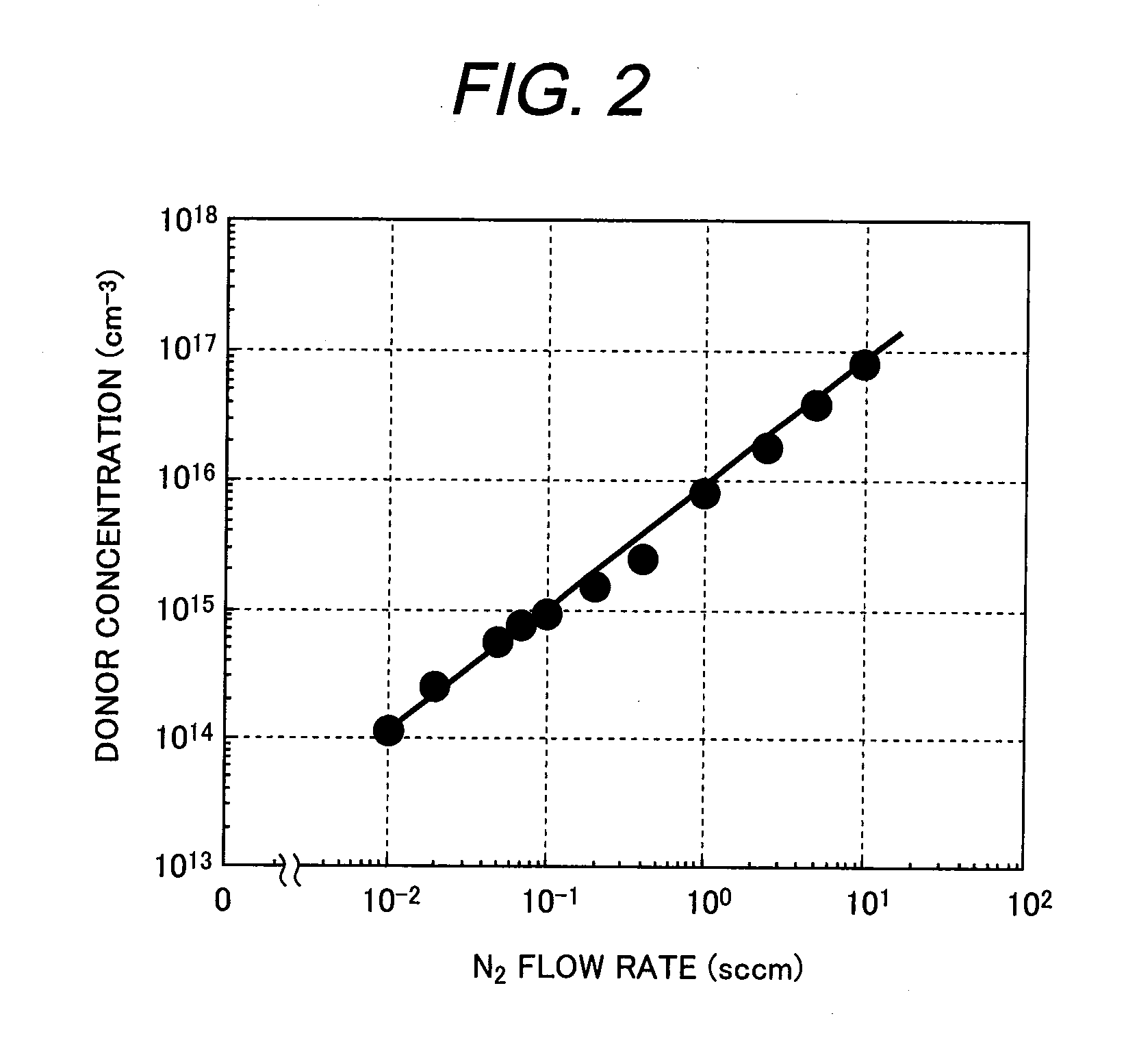
[0048]The basic mode of the present invention that includes a silicon carbide semiconductor substrate having a semiconductor layer of a low basal-plane dislocation density above a base substrate formed of a silicon carbide semiconductor single crystal is used as a first embodiment of the invention to study growth conditions for obtaining a low-donor-concentration silicon carbide epitaxial layer to be used as a dislocation conversion layer.

[0049]First, the base substrate formed of a silicon carbide single-crystal wafer is prepared for use. The silicon carbide single-crystal wafer is 4H—SiC with a 50-mm diameter n-type (0001) plane inclined by 8 degrees in a direction of [11-20]. The growth uses the Si-plane side of the wafer provided with chemical-mechanical polishing (CMP) after being mechanically polished into a mirror-like surface. This silicon carbide single-crystal wafer has a donor concentration of 3×1018 cm−3.

[0050]After being RCA-cleaned, the base substrate is set up in a sus...

second embodiment

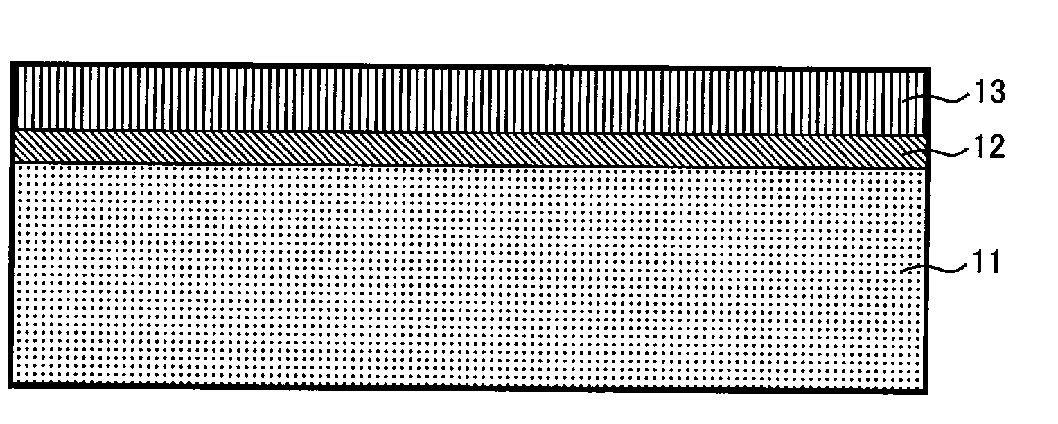
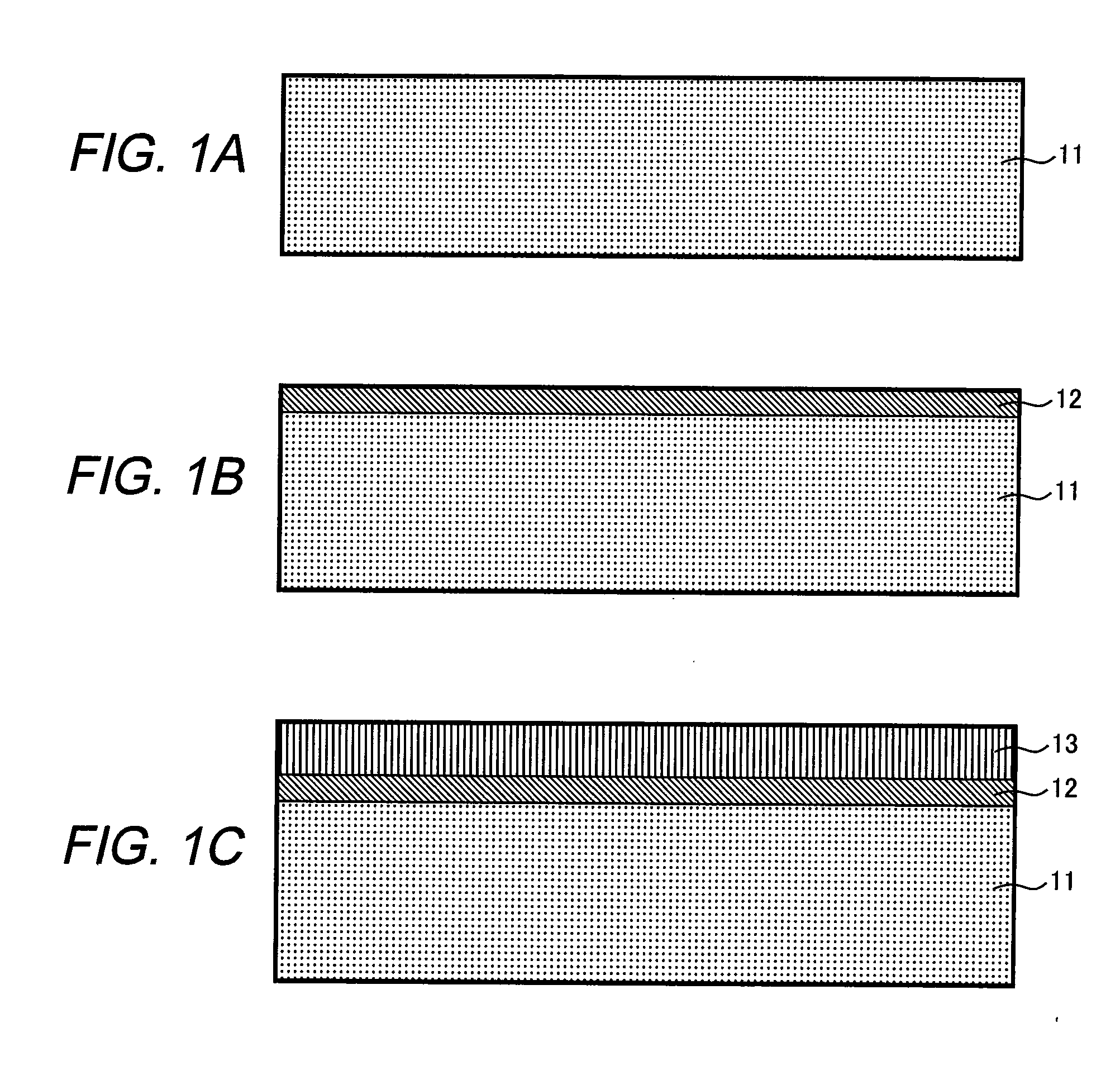
[0057]A method of manufacturing a silicon carbide semiconductor substrate usable for forming a semiconductor device will be described as a second embodiment of the present invention. The description is based on knowledge that was obtained from the foregoing fundamental experiments. FIGS. 1A to 1C are sectional views that show manufacturing process steps relating to the silicon carbide semiconductor substrate according to the present embodiment.

[0058]First, in the step shown in FIG. 1A, a base substrate 11 formed of a silicon carbide single-crystal wafer is prepared for use. The silicon carbide single-crystal wafer is 4H—SiC with a 50-mm diameter n-type (0001) plane inclined by 8 degrees in the direction of [11-20]. Growth of epitaxial layers uses the silicon-plane side of the wafer provided with a CMP process after being mechanically polished into a mirror-like surface. This silicon carbide single-crystal wafer has a donor concentration of ×1018 cm−3.

[0059]Next, in the step shown in...

third embodiment

[0074]A method of manufacturing a silicon carbide semiconductor substrate usable for forming a device and different from the semiconductor substrate of the second embodiment will be described as a third embodiment of the present invention. The description is based on the knowledge that was obtained in the first embodiment.

[0075]FIGS. 5A to 5D are sectional views that show manufacturing process steps relating to the silicon carbide semiconductor substrate according to the present embodiment.

[0076]First, in the step shown in FIG. 5A, a base substrate 51 formed of a silicon carbide single-crystal wafer is prepared for use. The silicon carbide single-crystal wafer is 4H—SiC with a 50-mm diameter n-type (0001) plane inclined by 8 degrees in the direction of [11-20]. Growth of epitaxial layers uses the silicon-plane side of the wafer provided with a CMP process after being mechanically polished into a mirror-like surface. This silicon carbide single-crystal wafer has a donor concentration...


PUM

PropertyMeasurementUnit
inclination angleaaaaaaaaaa
thicknessaaaaaaaaaa

Abstract

A manufacturing method is provided for a silicon carbide semiconductor substrate adapted for reduced basal plane dislocations in a silicon carbide epitaxial layer. Between a silicon carbide epitaxial layer for device fabrication (i.e., a drift layer) and a base substrate formed of a silicon carbide single-crystal wafer, a highly efficient dislocation conversion layer through which any basal plane dislocations in the silicon carbide single-crystal wafer are converted into threading edge dislocations very efficiently when the dislocations propagate into the layer epitaxially grown is provided by epitaxial growth. Assigning to the dislocation conversion layer a donor concentration lower than that of the drift layer, therefore, allows the above conversion of a larger number of basal plane dislocations than the case where the drift layer exists alone (without the dislocation conversion layer).

Description

CLAIM OF PRIORITY[0001]The present application claims priority from Japanese patent application JP 2007-255682 filed on Sep. 28, 2007, the content of which is hereby incorporated by reference into this application.BACKGROUND OF THE INVENTION[0002]1. Field of the Invention[0003]The present invention relates to a silicon carbide semiconductor substrate and a silicon carbide semiconductor device formed on the same.[0004]2. Description of the Related Art[0005]Silicon carbide (SiC), compared with silicon (Si), has a large bandgap and high breakdown field, so the application of silicon carbide to the next generation of semiconductor devices (power devices) for electric power control is anticipated. Silicon carbide is known to exhibit various crystal structures, which include the hexagonal 4H—SiC and 6H—SiC used to create practical power devices.[0006]Since a large portion of power devices need to supply a large current throughout their own internal circuits, these semiconductor devices ar...

Claims


Application Information

Patent Timeline
Patent Type & Authority Applications(United States)
IPC IPC(8): H01L29/24
CPCH01L21/02378H01L21/02447H01L21/02502H01L21/02529H01L21/02576H01L29/872H01L29/1608H01L29/32H01L29/6606H01L29/8611H01L21/0262
Inventor OHNO, TOSHIYUKIYOKOYAMA, NATSUKI
Owner HITACHI CABLE
Why Eureka
Try Eureka