Microstrip Lines with Tunable Characteristic Impedance and Wavelength

a microstrip line and characteristic impedance technology, applied in the direction of waveguides, printed circuits, electrical equipment, etc., can solve the problems of microstrip line ohmic losses becoming increasingly significant, microstrip line occupying a large chip area, and forming ground plane b>8/b> also incurs drawbacks

Active Publication Date: 2009-12-10
TAIWAN SEMICON MFG CO LTD
View PDF0 Cites 23 Cited by
  • Summary
  • Abstract
  • Description
  • Claims
  • Application Information

AI Technical Summary

Benefits of technology

[0036]The embodiments of the present invention have several advantageous features. Firstly, the characteristic impedance and characteristic wavelength may be tuned, and are not limited by the vertical distance between signal line and the underlying ground plane. Secondly, microstrip lines with greater characteristic impedances may be achieved without increasing the chip area of the microstrip lines. Thirdly, microstrip lines may have smaller characteristic wavelengths, resulting in shorter microstrip lines, which cause the further reduction in the chip area usage. Fourthly, the formation of the embodiments of the present invention do not need additional mask, and hence manufacturing cost is not increased.

Problems solved by technology

However, the formation of ground plane 8 also incurs drawbacks.
Consequently, ohmic losses in microstrip lines become increasingly more significant, and demand better impedance matching between microstrip line 2 and network devices.
In addition, microstrip lines typically occupy great chip area.
With the increasing down-scaling of integrated circuits, the chip-area requirement of the microstrip lines becomes a bottleneck preventing the integration of microwave devices and the integrated circuits adopting CMOS devices.

Method used


Image

  • Microstrip Lines with Tunable Characteristic Impedance and Wavelength
  • Microstrip Lines with Tunable Characteristic Impedance and Wavelength
  • Microstrip Lines with Tunable Characteristic Impedance and Wavelength

Examples


Embodiment Construction

[0019]The making and using of the presently preferred embodiments are discussed in detail below. It should be appreciated, however, that the present invention provides many applicable inventive concepts that can be embodied in a wide variety of specific contexts. The specific embodiments discussed are merely illustrative of specific ways to make and use the invention, and do not limit the scope of the invention.

[0020]Novel microstrip lines having tunable characteristic impedances and tunable characteristic wavelengths are provided. The variations of the preferred embodiments are then discussed. Throughout the various views and illustrative embodiments of the present invention, like reference numbers are used to designate like elements.

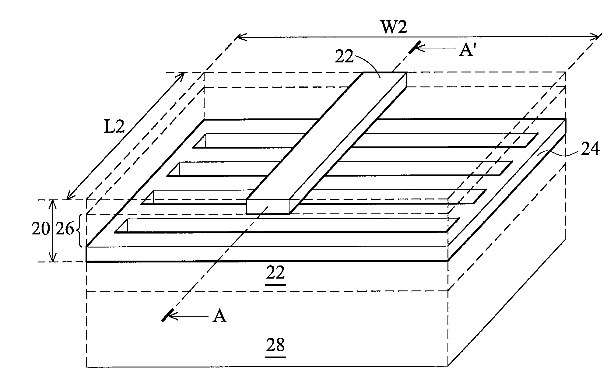
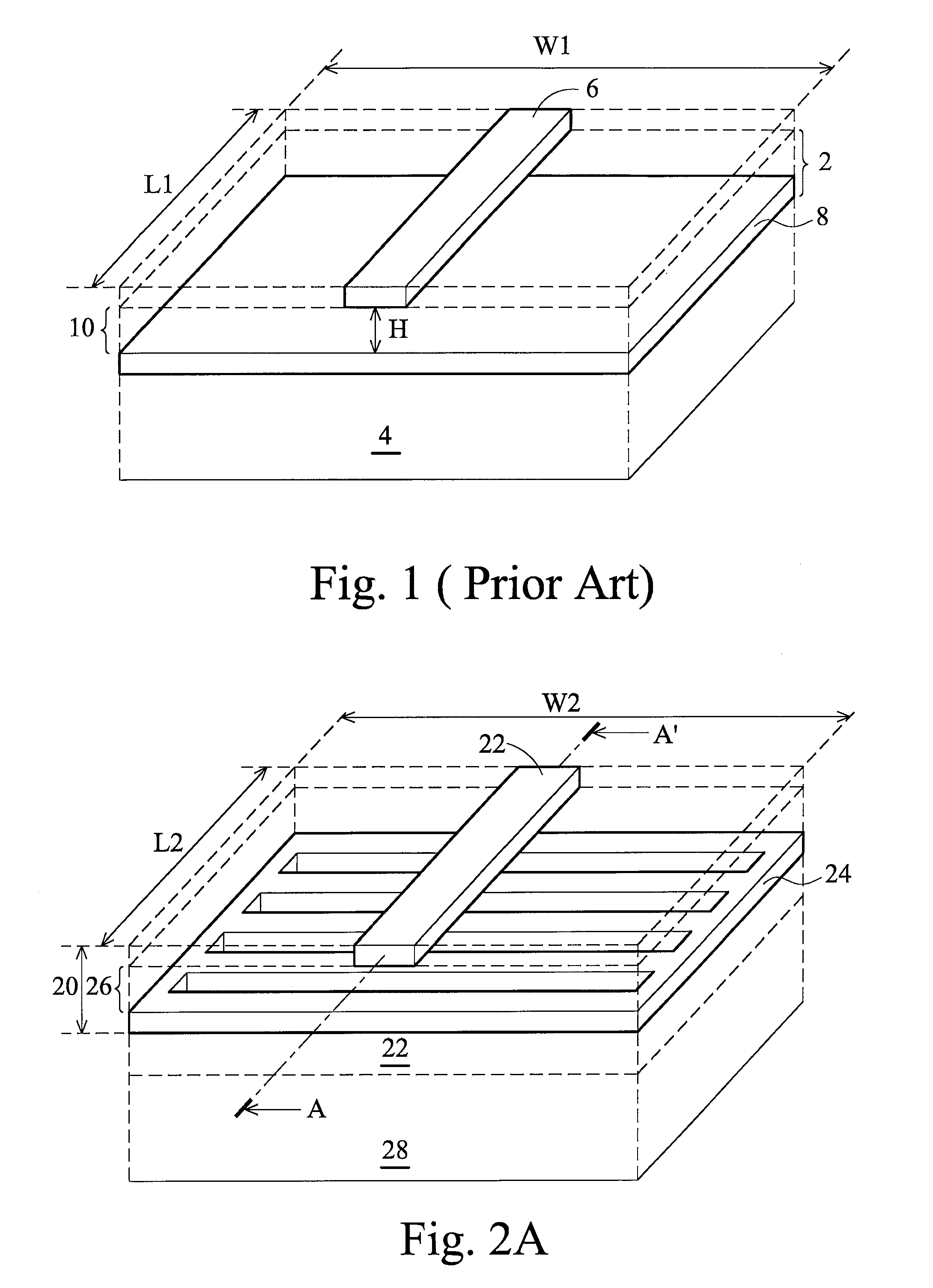
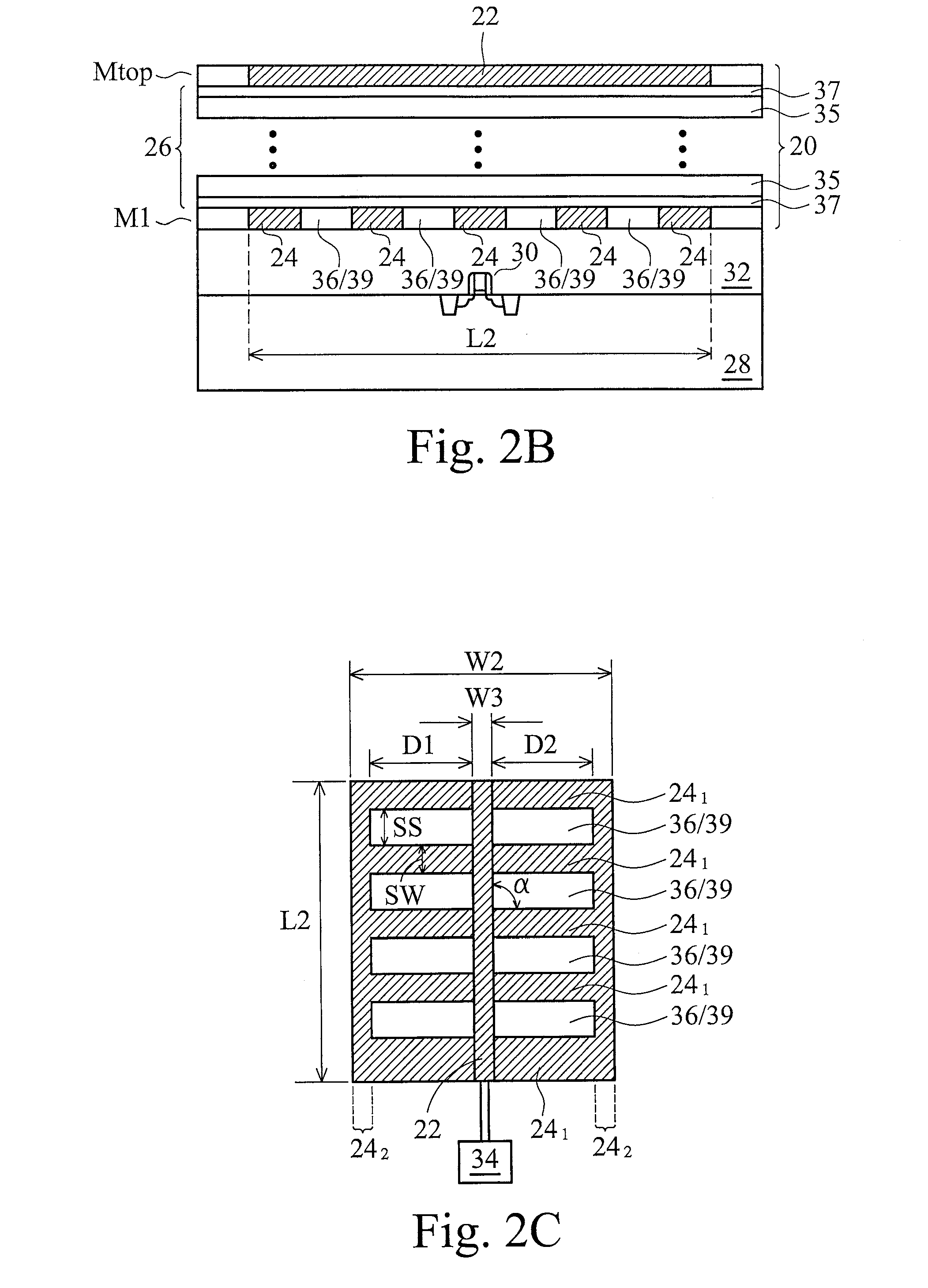
[0021]FIG. 2A illustrates a perspective view of an embodiment of the present invention. Microstrip line 20, which includes signal line 22, patterned ground plane 24, and dielectric layer(s) 26, is formed over substrate 28. In an embodiment, substrate 2...


PUM


Abstract

A microstrip line structure includes a conductive ground plane having a strip opening encircled by the ground plane. The strip opening extends from a top surface to a bottom surface of the ground plane. The microstrip line structure further includes a dielectric strip filling the strip opening; a dielectric layer over and contacting the ground plane; and a signal line over the dielectric layer, wherein the signal line has a portion directly above a portion of the dielectric strip, and wherein the signal line and the dielectric strip are non-parallel.

Description

TECHNICAL FIELD[0001]This invention relates generally to microstrip line structures, and more particularly to microstrip line structures having tunable characteristic impedances and tunable characteristic wavelengths.BACKGROUND[0002]Transmission lines are important elements in microwave circuit applications. These devices provide the interconnection between active and passive devices of microwave circuits, and are utilized as impedance matching elements as well. A microstrip line is a type of transmission line widely utilized in monolithic microwave integrated circuit (MMIC) applications.[0003]Microstrip lines have a number of advantages when utilized in MMIC applications. First of all, since microstrip lines are formed of conductive planes disposed on substrates, these devices are readily adaptable to the manufacturing process of the integrated circuits. Accordingly, microstrip lines may be integrated on a same substrate with commonly used integrated circuits such as complementary ...

Claims


Application Information

Patent Timeline
Patent Type & Authority Applications(United States)
IPC IPC(8): H01P3/08
CPCH01P3/082H05K1/0225H01P3/081
Inventor CHO, SHU-YING
Owner TAIWAN SEMICON MFG CO LTD
Why Eureka
Try Eureka