Semiconductor structure including gate electrode having laterally variable work function

a technology of lateral variable work function and semiconductor structure, which is applied in the direction of semiconductor devices, basic electric elements, electrical apparatus, etc., can solve the problems of high mosfet off-state current, insufficient level of electrical control of gate electrode, and high standby power consumption, and achieve effective work function

Active Publication Date: 2009-12-17
GLOBALFOUNDRIES US INC
View PDF15 Cites 6 Cited by
  • Summary
  • Abstract
  • Description
  • Claims
  • Application Information

AI Technical Summary

Benefits of technology

[0011]While not wishing to be bound to a particular theory of operation of a semiconductor structure in accordance with the invention, a threshold voltage of an n-FET or a p-FET may increase on increasing or decreasing a gate electrode work function thereof. If the n-FET or the p-FET has a higher or lower work function gate electrode on the edge compared to the center, then an effective work function would increase or decrease at smaller gate lengths of the gate electrode. Therefore, the n-FET or p-FET threshold voltage would increase at smaller gate lengths before short-channel effects overwhelm the above-mentioned work function related effect, thus leading to a peak in threshold voltage vs gate length characteristics, similar to that which is realized in conventional FETs by using halo doping.

Problems solved by technology

Particularly detrimental novel effects are short channel effects.
Short channel effects result from an inadequate level of electrical control of a gate electrode over a channel region within a MOSFET.
Undesirable results of short channel effects include high MOSFET off-state currents, high standby power consumptions, and detrimental electrical parameter variations within MOSFET devices.
However, while these undoped body regions provide MOSFET devices with enhanced short channel effect control, undoped body regions may in fact provide for compromise of other electrical parameters of MOSFET devices.

Method used


Image

  • Semiconductor structure including gate electrode having laterally variable work function
  • Semiconductor structure including gate electrode having laterally variable work function
  • Semiconductor structure including gate electrode having laterally variable work function

Examples


Embodiment Construction

[0020]The invention, which includes a semiconductor structure that in turn includes a gate electrode having a laterally variable work function (and methods for fabrication thereof), is described in greater detail below within the context of the drawings described above. Since the drawings are intended for illustrative purposes, the drawings are not necessarily drawn to scale.

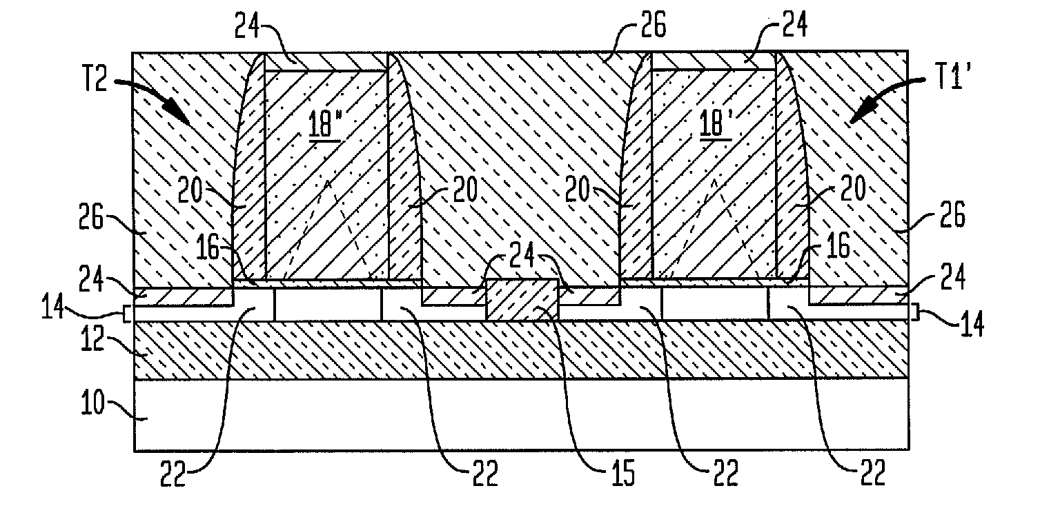
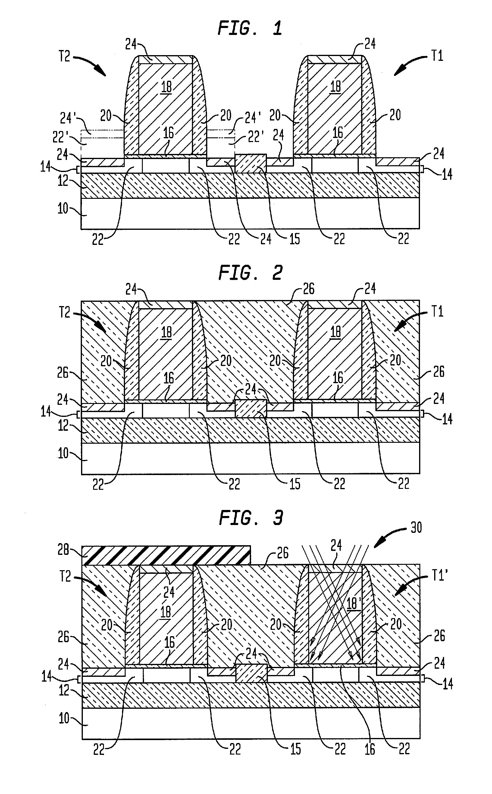
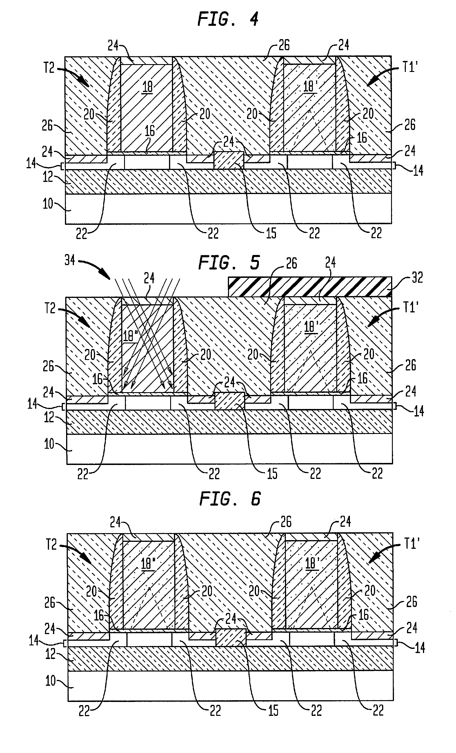
[0021]FIG. 1 to FIG. 6 show a series of schematic cross-sectional diagrams illustrating the results of progressive stages in fabricating a semiconductor structure in accordance with an embodiment of the invention. This particular embodiment of the invention comprises a first embodiment of the invention. FIG. 1 shows a schematic cross-sectional diagram of the semiconductor structure at an early stage in fabrication thereof in accordance with the first embodiment.

[0022]FIG. 1 shows a base semiconductor substrate 10. A buried dielectric layer 12 is located upon the base semiconductor substrate 10 and a surface semi...


PUM


Abstract

A semiconductor structure, such as a CMOS structure, includes a gate electrode that has a laterally variable work function. The gate electrode that has the laterally variable work function may be formed using an angled ion implantation method or a sequential layering method. The gate electrode that has the laterally variable work function provides enhanced electrical performance within an undoped channel field effect transistor device.

Description

RELATED APPLICATIONS[0001]This application is a divisional of U.S. application Ser. No. 11 / 677,207, filed Feb. 21, 2007.BACKGROUND[0002]1. Field of the Invention[0003]The invention relates generally to semiconductor structures that may include metal oxide semiconductor field effect transistor (MOSFET) devices. More particularly, the invention relates to semiconductor structures with enhanced performance.[0004]2. Description of the Related Art[0005]As MOSFET device dimensions decrease, and in particular as MOSFET gate electrode dimensions decrease, several novel effects become more prominent within MOSFET devices. Particularly detrimental novel effects are short channel effects. Short channel effects result from an inadequate level of electrical control of a gate electrode over a channel region within a MOSFET. Undesirable results of short channel effects include high MOSFET off-state currents, high standby power consumptions, and detrimental electrical parameter variations within MO...

Claims


Application Information

Patent Timeline
Patent Type & Authority Applications(United States)
IPC IPC(8): H01L29/78
CPCH01L21/26586H01L21/28026H01L21/28105H01L21/823842H01L21/823864H01L21/823878H01L29/785H01L29/4232H01L29/4908H01L29/4983H01L29/66545H01L29/66772H01L21/84
Inventor HAENSCH, WILFRIEDKOESTER, STEVENMAJUMDAR, AMLAN
Owner GLOBALFOUNDRIES US INC
Why Eureka
Try Eureka