Organic light emitting diodes with structured electrodes

a light-emitting diode and organic technology, applied in the field of electromechanical devices, can solve the problems of lcd energy waste, no light, no power consumption, no light, etc., and achieve the effect of plasma displays, and reducing the cost of lcds

Active Publication Date: 2010-05-27
RGT UNIV OF CALIFORNIA
View PDF4 Cites 7 Cited by
  • Summary
  • Abstract
  • Description
  • Claims
  • Application Information

AI Technical Summary

Problems solved by technology

OLEDs can be printed onto any suitable substrate using inkjet printer or even screen printing technologies, which can result in a significantly lower cost than LCDs or plasma displays.
LCDs use a backlight and cannot show true black, while an “off” OLED element produces no light and consumes no power.
Energy is wasted in LCDs because they require polarizers which filter out about half of the light emitted by the backlight.
The interface between the cathode and organic layers in OLEDs presents a barrier for electron ejection, which reduces electron ejection efficiency and can lead to a significantly large device operating voltage with reduced overall device efficiency.
Additionally, the barrier results in an increase in temperature at the interface which may damage the device.
Temperatures can reach over 100° C., which can cause severe damage to an OLED.
Another obstacle involves the stability of the OLED.
Exposure to the environment (e.g., heat, H2O and O2) can be particularly damaging, leading to marked deterioration in device performance.
Lastly, much of the light that is emitted by the organic molecules in an OLED remains trapped in the device and does not reach the viewer.
Although alkali or alkali earth metals display the lowest work function (2-3 eV) of all elemental metals, thus suitable for cathode applications, their reactive nature and the associated fabrication cost have been a major challenge for the realization of low cost, high efficient OLED devices.

Method used


Image

  • Organic light emitting diodes with structured electrodes
  • Organic light emitting diodes with structured electrodes
  • Organic light emitting diodes with structured electrodes

Examples


Embodiment Construction

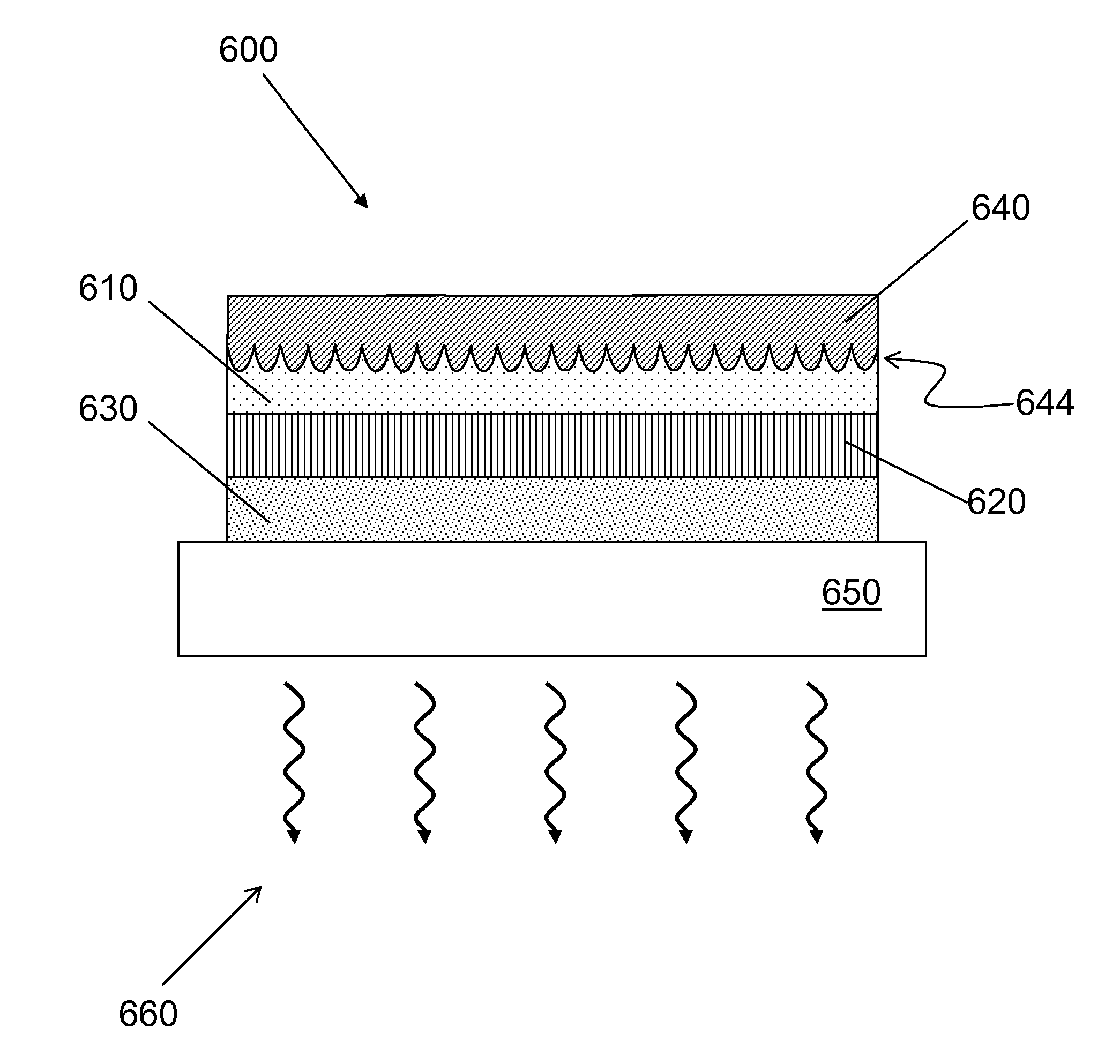
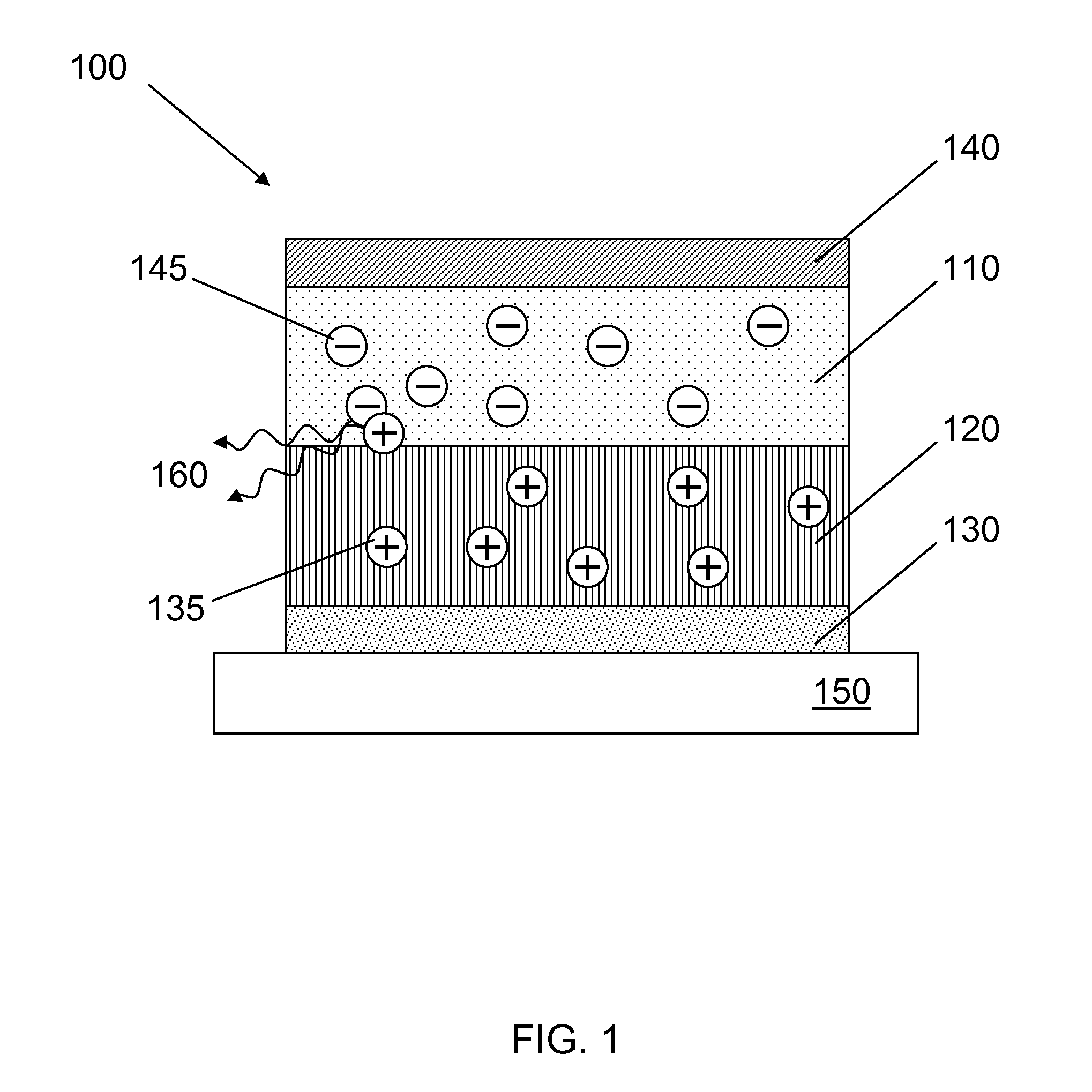
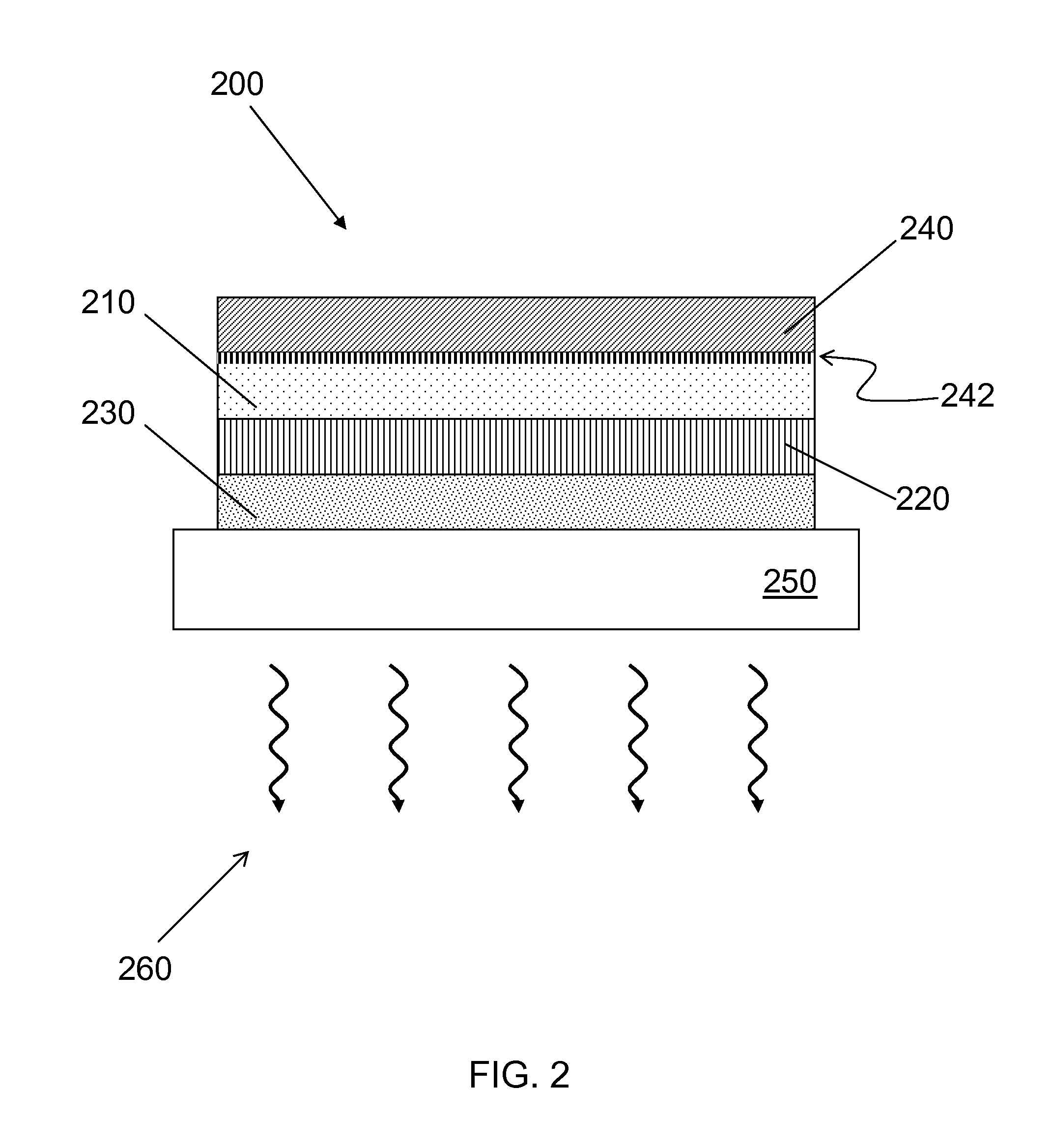
[0015]Embodiments are described herein in the context of organic light emitting diodes with structured electrodes. Those of ordinary skill in the art will realize that the following detailed description is illustrative only and is not intended to be limiting in any way. Other embodiments will suggest themselves readily to skilled persons having the benefit of this disclosure.

[0016]In the interest of clarity, not all of the routine features of the implementations described herein are shown and described. It will, of course, be appreciated that in the development of any such actual implementation, numerous implementation-specific decisions must be made in order to achieve the developer's specific goals, such as compliance with application- and business-related constraints, and that these specific goals will vary from one implementation to another and from one developer to another. Moreover, it will be appreciated that such a development effort might be complex and time-consuming, but ...


PUM

PropertyMeasurementUnit
work functionaaaaaaaaaa
wavelengthaaaaaaaaaa
radiiaaaaaaaaaa

Abstract

A cathode that contain nanostructures that extend into the organic layer of an OLED has been described. The cathode can have an array of nanotubes or a layer of nanoclusters extending out from its surface. In another arrangement, the cathode is patterned and etched to form protruding nanostructures using a standard lithographic process. Various methods for fabricating these structures are provided, all of which are compatible with large-scale manufacturing. OLEDs made with these novel electrodes have greatly enhanced electron injection, have good environmental stability.

Description

CROSS-REFERENCE TO RELATED APPLICATIONS[0001]This application claims priority to U.S. Provisional Patent Application 60 / 796,647, filed Apr. 26, 2006, which is incorporated by reference herein.STATEMENT OF GOVERNMENTAL SUPPORT[0002]The invention described and claimed herein was made in part utilizing funds supplied by the U.S. Department of Energy under Contract No. DE-AC02-05CH11231. The U.S. Government has certain rights in this invention.TECHNICAL FIELD[0003]The present invention relates to electronic devices that incorporate organic layers. More particularly, the present invention relates to structured cathodes for devices such as organic light emitting diodes (“OLEDs”), solar cells, and the like.BACKGROUND ART[0004]Efficient film devices, including organic photovoltaic and organic electroluminescent devices have been the subject of much advancement recently. In particular, organic light emitting small molecules and polymers have attracted increasing interest for manufacture of l...

Claims


Application Information

Patent Timeline
Patent Type & Authority Applications(United States)
IPC IPC(8): H01L51/52B32B3/00
CPCB82Y10/00H01L51/0018H01L51/0021Y10T428/24479H01L51/5203H01L51/5234H01L2251/5369H01L51/0048H10K71/233H10K71/60H10K85/221H10K50/805H10K50/828H10K2102/331H05B33/06H05B33/10H05B33/26
Inventor MAO, SAMUEL S.LIU, GAOJOHNSON, STEPHEN G.
Owner RGT UNIV OF CALIFORNIA
Why Eureka
Try Eureka