
Method and apparatus for manufacturing semiconductor device

a semiconductor and manufacturing technology, applied in the direction of transistors, vacuum evaporation coatings, coatings, etc., can solve the problems of deteriorating leak current characteristics, affecting the efficiency of semiconductor devices, and unable to achieve desired effective work functions, etc., to achieve effective work functions, improve leak current characteristics, and increase eot

Active Publication Date: 2013-07-09
CANON ANELVA CORP
View PDF30 Cites 2 Cited by
  • Summary
  • Abstract
  • Description
  • Claims
  • Application Information

AI Technical Summary

Benefits of technology

The present invention provides a method and apparatus for manufacturing a semiconductor device using the PVD method that can achieve a desired effective work function and minimize leak current without increasing equivalent oxide thickness. This results in improved performance of the semiconductor device without adding extra layers of material.

Problems solved by technology

However, it is conceivable that transistor characteristics deteriorate due to impurities contained in a material of the electrode, as shown in Non-patent Document 2.
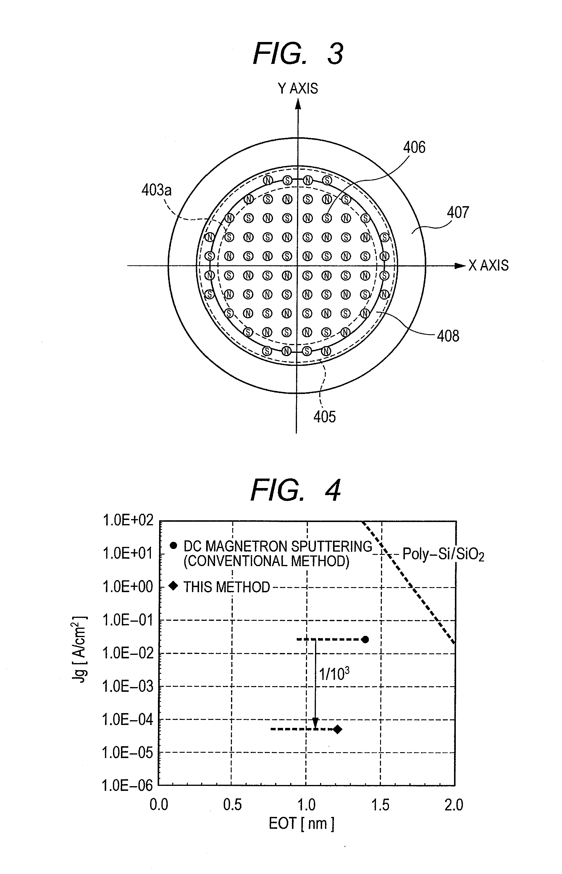
On the other hand, the PVD method possibly causes a smaller amount of impurities to be mixed in the material than the CVD method does, but has problems that the leak current characteristics deteriorate and a desired effective work function cannot be obtained unlike the CVD method, as shown in Non-patent Document 3.
However, this method is becoming inadequate with advancement of the miniaturization of transistors (a gate length of 32 nm or smaller).

Method used


Image

  • Method and apparatus for manufacturing semiconductor device
  • Method and apparatus for manufacturing semiconductor device
  • Method and apparatus for manufacturing semiconductor device

Examples


first example

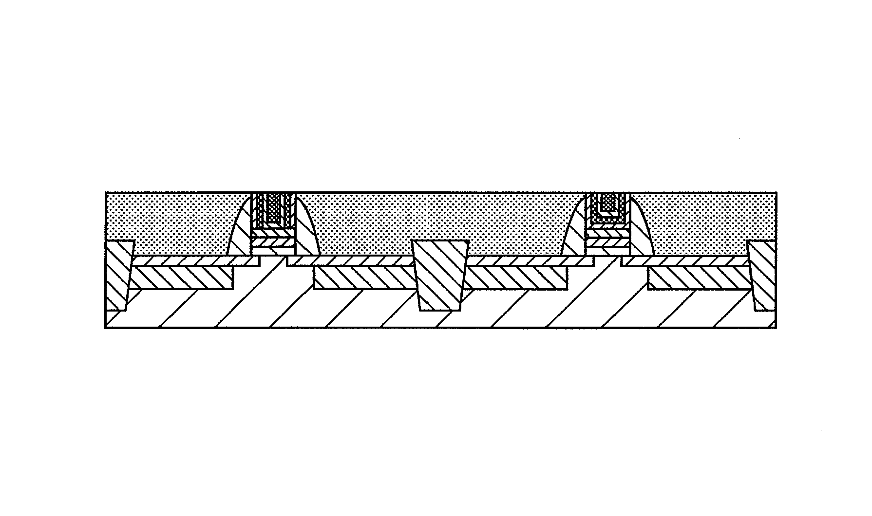
[0063]A first example of the present invention will be described in detail with reference to the drawings. FIGS. 7A to 7C are diagrams showing a process of a method for manufacturing a semiconductor device according to the first example of the present invention. First, as shown in FIG. 7A, an element isolation region 502 formed by the STI (Shallow Trench Isolation) technology was provided on a surface of a silicon substrate 501. Subsequently, a silicon thermally-oxidized film of 1.0 nm thickness was formed by a thermal oxidation method on the surface of the silicon substrate 501 subjected to element isolation. Then, the silicon substrate 501 was put in a cluster tool 600 shown in FIG. 8. In FIG. 8, the silicon substrate 501 was first delivered from a road lock chamber 605 to a chamber 601, and then Hf of 0.5 nm to 0.7 nm thickness was deposited on the silicon substrate 501 by a sputtering method. Next, the silicon substrate 501 on which Hf was formed was delivered to a chamber 602 t...

second example

[0065]A second example of the present invention will be described below with reference to the drawings. FIGS. 9A to 9G are diagrams showing a process of a method for manufacturing a semiconductor device according to the second example of the present invention. First, as shown in FIG. 9A, an element isolation region 702 was formed on a surface of a silicon substrate 701 by the STI technology. Subsequently, a silicon thermally-oxidized film 703 of 1.0 nm thickness was formed by a thermal oxidation method on the surface of the silicon substrate 701 subjected to element isolation, and thereafter a high-permittivity film 704 made of HfO2 was formed with a thickness of 2.0 nm by a CVD method, an ALD method, or a sputtering method, whereby a high-permittivity gate insulating film 705 containing the high-permittivity film was formed.

[0066]Next, a titanium nitride film 706 of 2.0 nm thickness was formed on the high-permittivity gate insulating film 705 by the same method as in the first exam...

third example

[0070]A third example of the present invention will be described below with reference to the drawings. FIGS. 11A to 11F are diagrams showing a process of a method for manufacturing a semiconductor device according to the third example of the present invention. In this example, the “step of forming the trench structure” in the second example is carried out in each of a region for forming a n-type MOSFET being a first region and a region for forming a p-type MOSFET being a second region to form a metal gate electrode achieving an effective work function suitable for the corresponding MOSFET.

[0071]As shown in FIG. 11A, trench structures 801 and 802 were formed in the first region for forming the n-type MOSFET and the second region for forming the p-type MOSFET, respectively, by using the same method as in the second example.

[0072]Next, as shown in FIG. 11B, a tantalum nitride film 803 and a titanium nitride film 804 were formed to cover the inside of the trench structures, by using the...


PUM

PropertyMeasurementUnit
pressureaaaaaaaaaa
pressureaaaaaaaaaa
frequencyaaaaaaaaaa

Abstract

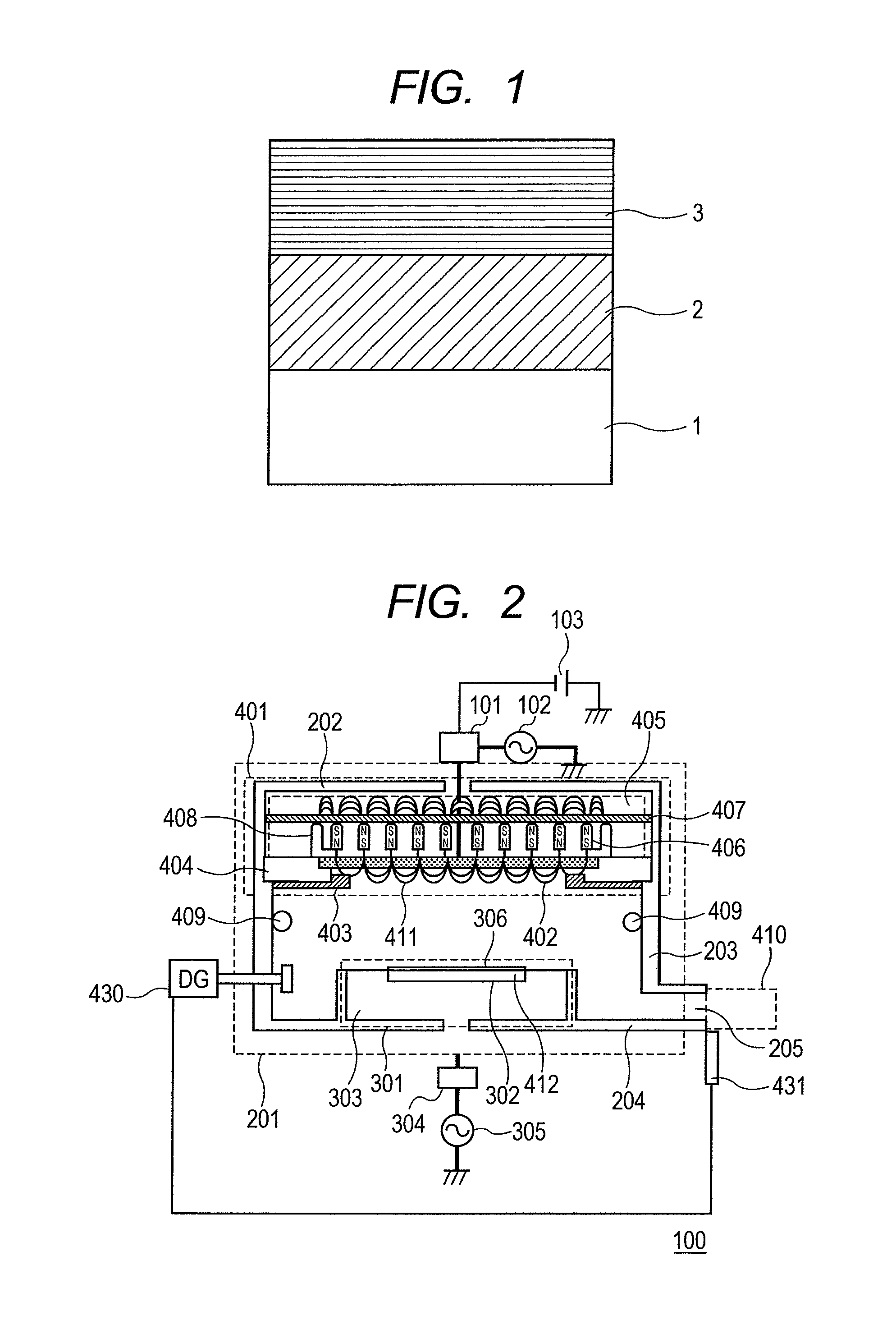
The present invention provides a method and apparatus for manufacturing a semiconductor device using a PVD method and enabling achievement of a desired effective work function and reduction in leak current without increasing an equivalent oxide thickness. A method for manufacturing a semiconductor device in an embodiment of the present invention includes the steps of: preparing a substrate on which an insulating film having a relative permittivity higher than that of a silicon oxide film is formed; and depositing a metal nitride film on the insulating film. The metal nitride depositing step is a step of sputtering deposition in an evacuatable chamber using a metal target and a cusp magnetic field formed over a surface of the metal target by a magnet mechanism in which magnet pieces are arranged as grid points in such a grid form that the adjacent magnet pieces have their polarities reversed from each other.

Description

CROSS-REFERENCES TO RELATED APPLICATIONS[0001]This application is a continuation application of International Application No. PCT / JP2011 / 007292, filed Dec. 27, 2011, which claims the benefit of Japanese Patent Application No. 2010-294008, filed Dec. 28, 2010. The contents of the aforementioned applications are incorporated herein by reference in their entireties.BACKGROUND OF THE INVENTION[0002]1. Field of the Invention[0003]The present invention relates to a method and apparatus for manufacturing a semiconductor device including a high-permittivity insulating film and a metal gate electrode. The present invention particularly relates to technology for enhancing performance of MOSFETs (Metal Oxide Semiconductor Field Transistor).[0004]2. Description of the Related Art[0005]Advanced CMOS (complementary MOS) device development with increasing miniaturization of transistors faces problems of a deterioration of drive current due to a depletion of a polysilicon (Poly-Si) electrode and an...

Claims


Application Information

Patent Timeline
Patent Type & Authority Patents(United States)
IPC IPC(8): H01L21/285H01L29/66
CPCC23C14/04H01J37/3455C23C14/351C23C14/54H01J37/34H01J37/345H01J37/3452H01L21/823842H01L29/4966H01L29/513H01L29/517H01L29/518H01L29/66545H01L29/6659H01L29/7833H01L21/28556H01L29/66477C23C14/0641H01L21/2855H01L21/823864
Inventor KITANO, NAOMUSEINO, TAKUYAMATSUO, AKIRASATO, YUMORIMOTO, EITARO
Owner CANON ANELVA CORP
Learn More