Radiation detection apparatus and radiographic imaging system

a detection apparatus and radiographic imaging technology, applied in the direction of x/gamma/cosmic radiation measurement, instruments, radiofrequency controlled devices, etc., can solve the problems of increasing noise, deteriorating quality, increasing noise, etc., and achieve satisfactory image and reduce unevenness.

Active Publication Date: 2010-01-07
CANON KK
View PDF26 Cites 17 Cited by
  • Summary
  • Abstract
  • Description
  • Claims
  • Application Information

AI Technical Summary

Benefits of technology

[0009]The present invention provides a radiation detection apparatus which can reduce unevenness of an image attributed to the thickness distribution of an interlayer insulation film, and obtain a satisfactory image by stabilizing the characteristic of a sensor element on the interlayer insulation film.

Problems solved by technology

In a radiation detection apparatus, as the parasitic capacitance of a signal line increases, the amount of noise, in turn, increases.
However, in such an arrangement, the image obtained when the interlayer insulation film has a thickness as small as, for example, 500 nm is more likely to have unevenness, which deteriorates its quality, than that obtained when the interlayer insulation film has a large thickness.

Method used


Image

  • Radiation detection apparatus and radiographic imaging system
  • Radiation detection apparatus and radiographic imaging system
  • Radiation detection apparatus and radiographic imaging system

Examples


first embodiment

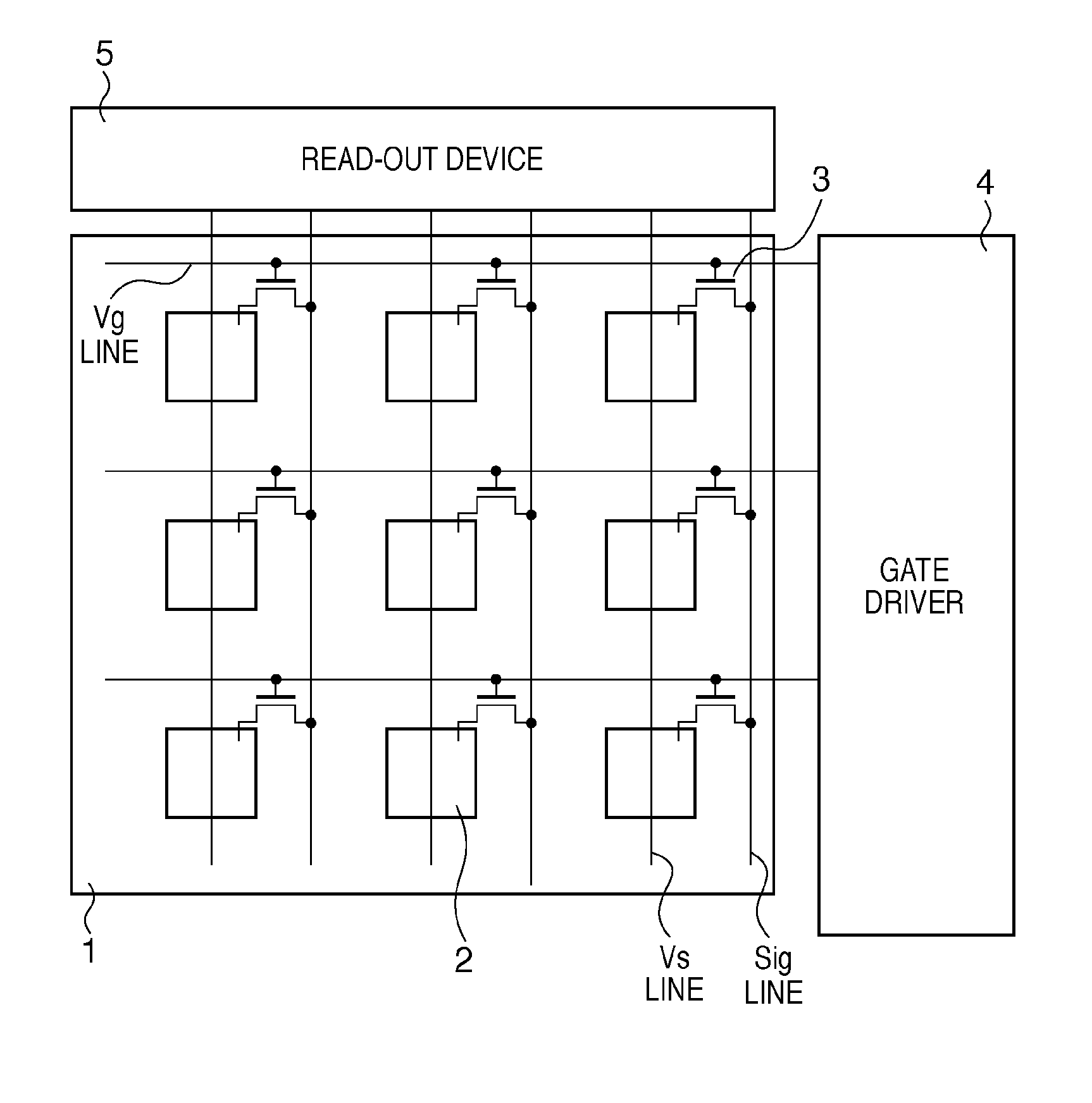
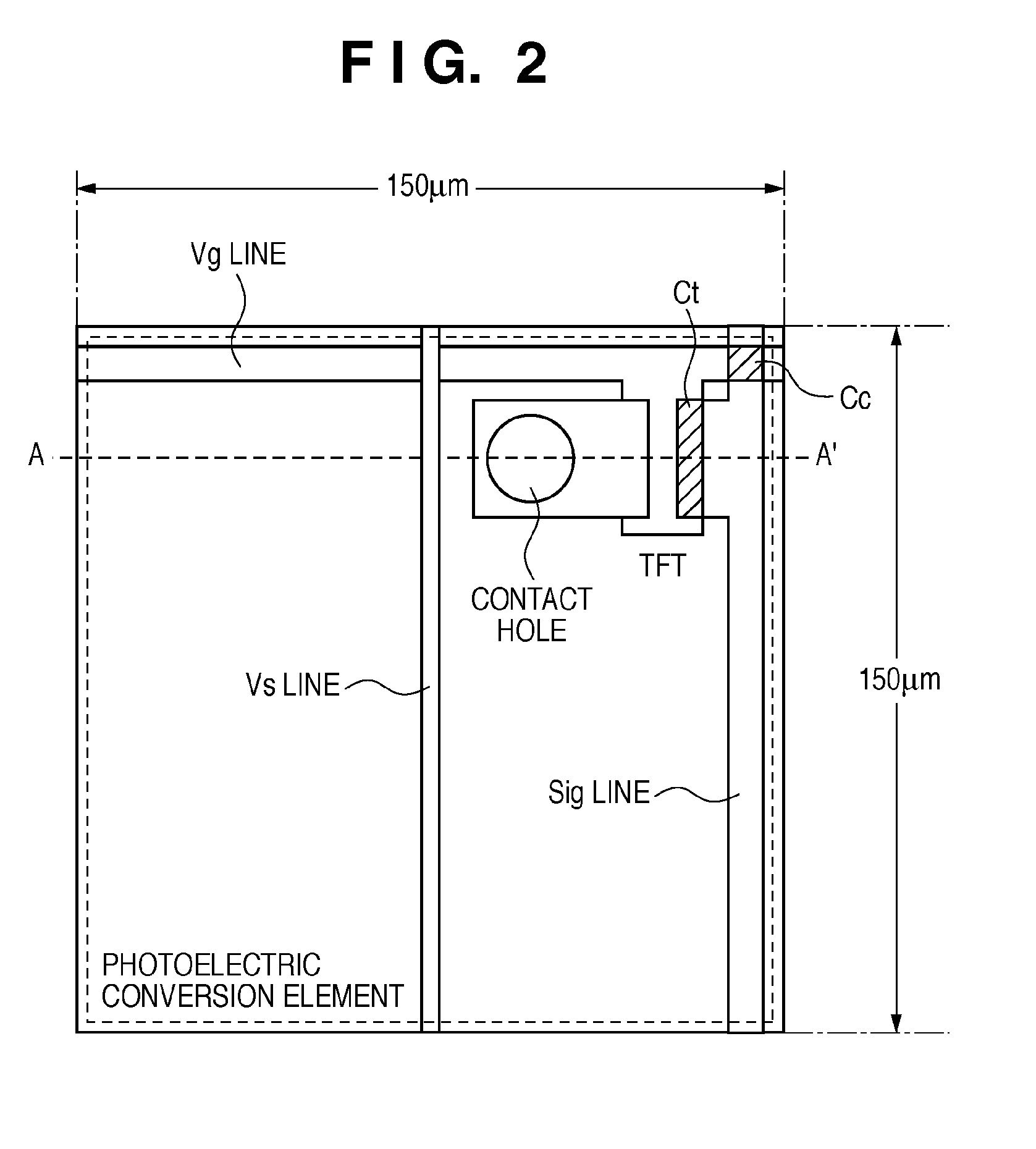
[0027]FIG. 1 is a circuit diagram showing the circuitry of a radiation detection apparatus according to the first embodiment of the present invention. FIG. 2 is a plan view showing one pixel. FIG. 3 is a sectional view taken along a line A-A′ in FIG. 2. FIG. 4 is a correlation graph showing the relationships between the thickness of an interlayer insulation film and the capacitances added to a signal line. FIG. 5 is a sectional view showing a contact hole to connect a conversion element and a switching element.

[0028]As shown in FIG. 1, a plurality of pixels each including a conversion element 2 and switching element 3 are arrayed in a matrix in a radiation detection panel 1 serving as a radiation detection apparatus. An MIS type photoelectric conversion element, for example, is used as the conversion element 2. The switching element 3 is a signal transfer switching element which transfers the signal from the conversion element 2. The gate of the switching element 3 is connected to a...

second embodiment

[0059]The second embodiment of the present invention will be explained next. FIG. 7 is a circuit diagram showing the circuitry according to this embodiment. FIG. 8 is a plan view showing one pixel. FIG. 9 is a sectional view taken along a line B-B′ in FIG. 8. FIG. 10 is a correlation graph showing the relationships between the thickness of an interlayer insulation film and the capacitances added to a signal line. The same reference numerals as in FIGS. 1 to 3 denote the same parts in FIGS. 7 to 9.

[0060]In this embodiment, one pixel includes a conversion element (photoelectric conversion element) 2, a signal transfer TFT 3 serving as a signal transfer switching element, and a reset TFT 6 serving as a reset switching element. One pixel also includes a gate line (Vr line) and reset line (Vt line) in addition to a bias line (Vs line), gate line (Vg line), and signal line (Sig line).

[0061]A plurality of pixels as described above are arrayed in a matrix in a radiation detection panel 1. A...

third embodiment

[0083]The third embodiment of the present invention will be explained next. FIG. 11 is a plan view showing one pixel. FIG. 12 is a sectional view taken along a line C-C′ in FIG. 11. The same reference numerals as in FIGS. 1 to 3 denote the same parts in FIGS. 11 and 12.

[0084]The arrangement of one pixel will be explained with reference to FIG. 11. A photoelectric conversion element serving as a conversion element 2, and a TFT serving as a switching element 3 are arranged in one pixel of a radiation detection panel, as in the first embodiment. Also, an Sig line, a Vg line, and a Vs line are formed in one pixel. The third embodiment is different from the first embodiment in that a contact hole to connect the photoelectric conversion element and the TFT has a rectangular or elliptical shape.

[0085]The arrangement of one pixel in this embodiment will be explained with reference to FIG. 12. FIG. 12 is a sectional view taken along a line C-C′ in FIG. 11. Referring to FIG. 12, reference num...


PUM


Abstract

A radiation detection apparatus comprises a plurality of pixels each including a conversion element which converts incident radiation into a charge, a switching element which transfers the charge, and an interlayer insulation film disposed between the conversion element and the switching element, a gate line to drive the switching element, and a signal line located to intersect with the gate line and configured to read out the charge transferred from the switching element, wherein Ca≧ε0×ε×S/d and 7d≦P/2 is satisfied, where P is a pixel pitch, Ca is a sum total of coupling capacitances between the signal line and the gate line, S is an overlapping area of the signal line and the conversion element, d is a thickness of the interlayer insulation film, ε is a relative dielectric constant of the interlayer insulation film, and ε0 is a vacuum dielectric constant.

Description

BACKGROUND OF THE INVENTION[0001]1. Field of the Invention[0002]The present invention relates to a radiation detection apparatus and radiographic imaging system which can be used in, for example, a medial image diagnostic apparatus, a nondestructive inspection apparatus, and an analysis apparatus using radiation.[0003]2. Description of the Related Art[0004]In recent years, as a technique for manufacturing a liquid crystal display panel using a thin-film transistor (TFT) makes advance, the sizes of both the panel and the screen of its display unit increase. This manufacturing technique is applied to a wide area sensor including a photoelectric conversion element or a direct conversion element which directly converts radiation such as X-rays into a charge, and a switching element such as a TFT. An area sensor including a photoelectric conversion element is often used in the field of radiation detection apparatuses such as a medical X-ray detection apparatus in combination with a scint...

Claims


Application Information

Patent Timeline
Patent Type & Authority Applications(United States)
IPC IPC(8): G01T1/24
CPCG01T1/2018G01T1/2006
Inventor ISHII, TAKAMASAMOCHIZUKI, CHIORIWATANABE, MINORU
Owner CANON KK
Why Eureka
Try Eureka