Method for forming p-type lightly doped drain region using germanium pre-amorphous treatment

a technology of germanium pre-amorphous treatment and drain region, which is applied in the direction of semiconductor devices, electrical equipment, transistors, etc., can solve the problems of high cost of integrated circuit or chip fabrication facilities, difficult devices, and limited process use in integrated fabrication facilities, so as to reduce the transient enhanced diffusion profile, the effect of reducing the cost of integrated circuit or chip fabrication and high device yield per wafer

Active Publication Date: 2010-01-07
SEMICON MFG INT (SHANGHAI) CORP +1
View PDF9 Cites 17 Cited by
  • Summary
  • Abstract
  • Description
  • Claims
  • Application Information

AI Technical Summary

Benefits of technology

[0009]Many benefits are achieved by way of the present invention over conventional techniques. For example, the present technique provides an easy to use process that relies upon conventional technology. In a specific embodiments, the present method allows for an LDD region having a reduced transient enhanced diffusion profile. In some embodiments, the method provides higher device yields in dies per wafer. In some embodiments, the method provides MOS devices having improved threshold leakage current, Idsat, and Ioff, among others. Additionally, the method provides a process that is compatible with conventional process technology without substantial modifications to conventional equipment and processes. Depending upon the embodiment, one or more of these benefits may be achieved. These and other benefits will be described in more throughout the present specification and more particularly below.

Problems solved by technology

An integrated circuit or chip fabrication facility can cost hundreds of millions, or even billions, of U.S. dollars.
Making devices smaller is very challenging, as each process used in integrated fabrication has a limit.

Method used


Image

  • Method for forming p-type lightly doped drain region using germanium pre-amorphous treatment
  • Method for forming p-type lightly doped drain region using germanium pre-amorphous treatment
  • Method for forming p-type lightly doped drain region using germanium pre-amorphous treatment

Examples


Embodiment Construction

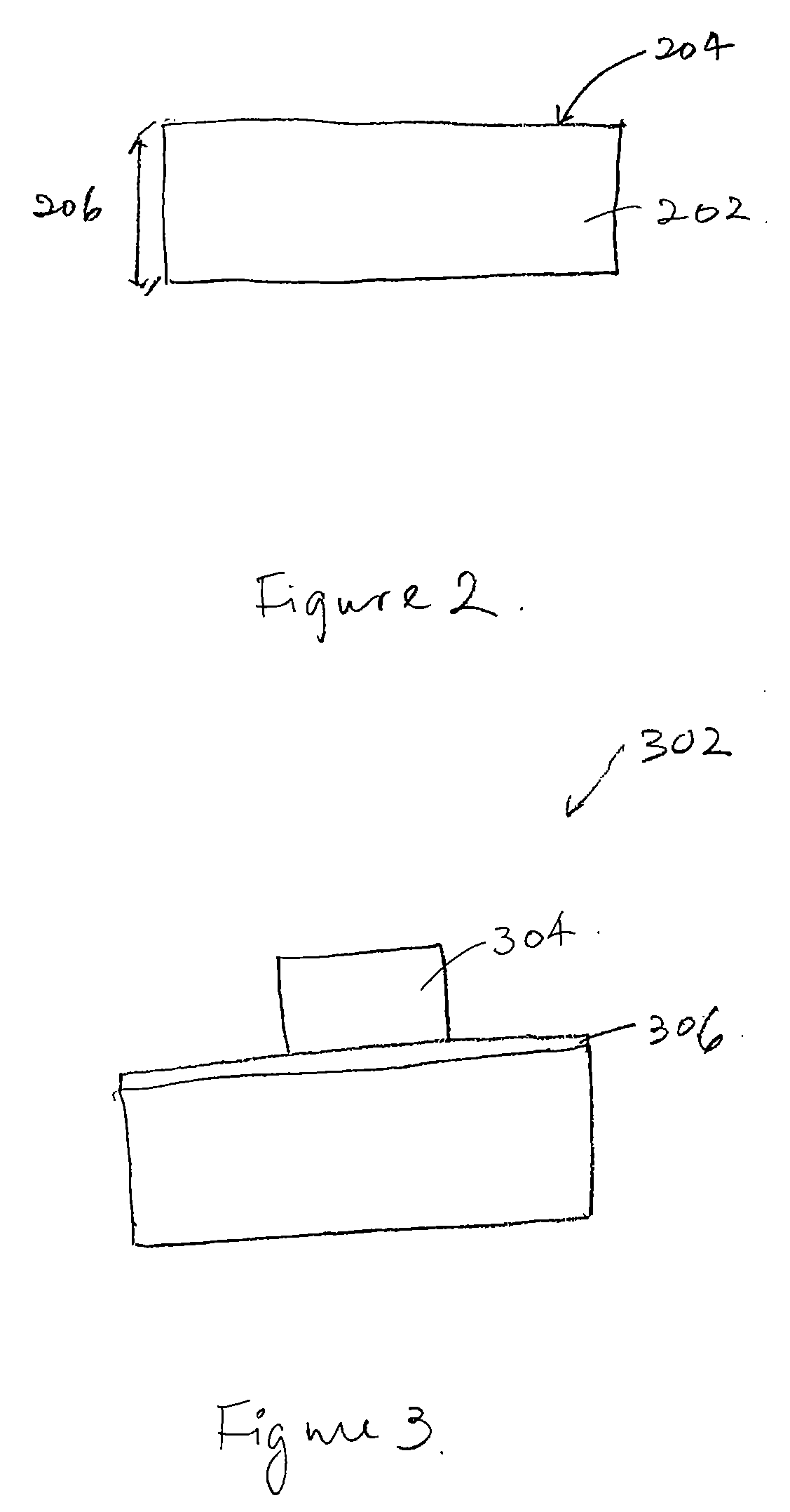
[0015]According to the present invention, techniques including methods and resulting structures for manufacture of semiconductor devices are provided. More particularly, the invention provides a method and device structure for forming an ultra shallow junction MOS device for the manufacture of integrated circuits. Merely by way of example, the invention has been applied to manufacturing of an ultra shallow junction MOS device using an ultra shallow lightly doped drain geometry. The present invention has been applied to manufacturing of a MOS structure having a line width of 65 nm and less. But it would be recognized that the present invention has a broader range of applicability.

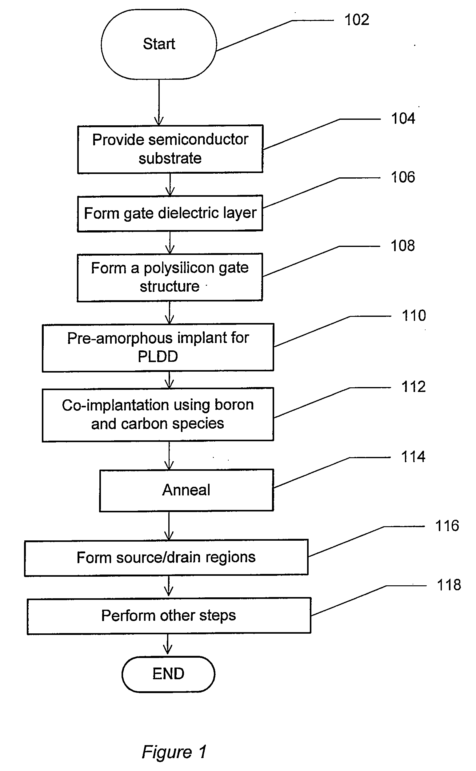
[0016]FIG. 1 is a simplified process flow diagram illustrating a method for forming a P doped lightly doped drain structure according to an embodiment of the present invention. The method starts with a Start step (Step 102). The method includes providing a semiconductor substrate (Step 104) having a surface ...


PUM


Abstract

A method for forming a MOS device with an ultra shallow lightly doped diffusion region. The method includes providing a semiconductor substrate including a surface region. The method provides a gate dielectric layer overlying the surface region and forms a gate structure overlying a portion of the gate dielectric layer. The method includes performing a first implant process using a germanium species to form an amorphous region within a lightly doped drain region in the semiconductor substrate using the gate structure as a mask. In a specific embodiment, the method includes performing a second implant process in the lightly doped drain region using a P type impurity and a carbon species using the gate structure as a mask. The method includes performing a first thermal process to activate the P type impurity in the lightly doped drain region. The method includes forming side wall spacers overlying a portion of the gate structure and performing a third implant process using a first impurity to form active source / drain regions in a vicinity of the surface region of the semiconductor substrate adjacent to the gate structure using the gate structure and the side wall spacer as a masking layer. The method then performs a second thermal process to activate the first impurity in the active source / drain regions.

Description

CROSS-REFERENCE TO RELATED APPLICATIONS[0001]This application claims priority to Chinese Patent Application No. 200810040289.4, filed Jul. 3, 2008, commonly assigned, and incorporated herein by reference for all purposes.BACKGROUND OF THE INVENTION[0002]The present invention is directed to integrated circuits and their processing for the manufacture of semiconductor devices. More particularly, the invention provides a method and a structure for manufacturing a MOS device having a ultra shallow lightly doped drain regions. But it would be recognized that the invention has a much broader range of applicability.[0003]Integrated circuits have evolved from a handful of interconnected devices fabricated on a single chip of silicon to millions of devices. Conventional integrated circuits provide performance and complexity far beyond what was originally imagined. In order to achieve improvements in complexity and circuit density (i.e., the number of devices capable of being packed onto a gi...

Claims


Application Information

Patent Timeline
Patent Type & Authority Applications(United States)
IPC IPC(8): H01L21/336
CPCH01L21/2236H01L29/7833H01L29/6659H01L21/26506H01L21/2658H01L21/2652
Inventor LEE, CHIA HAO
Owner SEMICON MFG INT (SHANGHAI) CORP
Why Eureka
Try Eureka