
Substrate bias switching unit for a low power processor

a switching unit and low-power processor technology, applied in the direction of climate sustainability, process and machine control, liquid/fluent solid measurement, etc., can solve the problems of increasing the static power consumption due to the leakage current, which was not conventionally large so much, and the static power consumption cannot be reduced. , to achieve the effect of reducing the leakage current and high speed

Inactive Publication Date: 2010-01-07
RENESAS ELECTRONICS CORP
View PDF23 Cites 1 Cited by
  • Summary
  • Abstract
  • Description
  • Claims
  • Application Information

AI Technical Summary

Benefits of technology

This approach enables high-speed operation while reducing power consumption by effectively managing substrate biases and clock signals, preventing malfunctions during mode transitions and minimizing leakage current, thus achieving efficient power management.

Problems solved by technology

However, the static power consumption due to the leakage current can not be reduced and hence still remains.
However, since if the threshold voltage is reduced, then the leakage current is remarkably increased, along with the reduction of the power source voltage, the increase of the static power consumption due to the leakage current which was not conventionally large so much becomes remarkable.
For this reason, it becomes a problem to realize a microprocessor in which the high speed is compatible with the low power consumption.

Method used


Image

  • Substrate bias switching unit for a low power processor
  • Substrate bias switching unit for a low power processor
  • Substrate bias switching unit for a low power processor

Examples


first embodiment

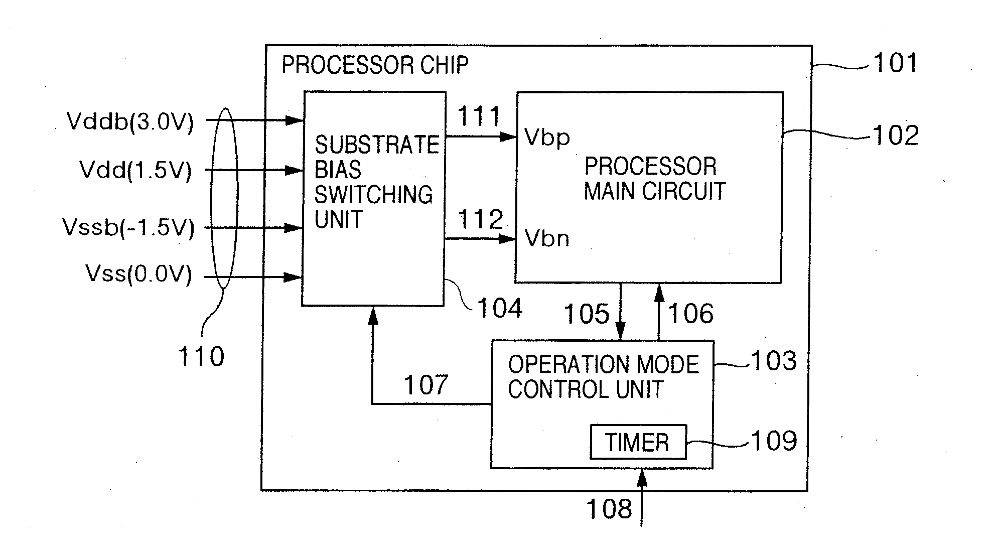
[0052]FIG. 1 is a block diagram showing an example of a configuration of a processor chip for realizing the present invention. In FIG. 1, a processor chip 101 is an LSI having a circuit of a CMOS structure, and includes a processor main circuit 102, an operation mode control unit 103, and a substrate bias switching unit 104. To the substrate bias switching unit 104, voltages Vdd and Vss in the normal mode, and voltages Vddb and Vssb in the stand-by mode are inputted through a signal 110. In accordance with a signal 107 outputted by the operation mode control unit, the substrate bias switching unit 104 selects, as the substrate bias for a p-channel MOS transistor constituting the processor main circuit 102, between Vdd and Vddb to output the selected one to a signal Vbp 111, and also selects, as the substrate bias for an n-channel MOS transistor, between Vss and Vssb to output the selected one to a signal Vbn 112. As for the voltage values for the substrate bias selection, for exampl...

third embodiment

[0063]FIG. 6 is a block diagram showing a configuration of a processor chip in the present invention. As for the basic device structure of a processor chip 601, the triple well structure as shown in FIG. 3 is assumed. In the processor chip 601 of FIG. 6, the processor main circuit includes a CPU 604, and a plurality of functional modules such as a module A 606 and a module B 608. The functional modules are present separately on the respective different well regions and hence one functional module is not influenced by the substrate bias control for other functional modules. The functional module includes the elements, each having the smaller scale unit, such as a CPU, an FPU, a cache, or a computing element. Substrate bias switching units 605, 607 and 609 are respectively provided so as to correspond to the functional modules 604, 606 and 608, and can switch, similarly to the above-mentioned embodiments, the substrate biases of the corresponding functional modules. The execution of t...


PUM

PropertyMeasurementUnit
time periodaaaaaaaaaa
voltageaaaaaaaaaa
voltageaaaaaaaaaa

Abstract

The feature of the present invention consists in: a processor main circuit for executing program instruction strings on a processor chip; a substrate bias switching unit for switching voltages of substrate biases applied to a substrate of the processor main circuit; and an operation mode control unit for controlling, in response to the execution of an instruction to proceed to a stand-by mode in the processor main circuit, the substrate bias switching unit in such a way that the biases are switched over to voltages for the stand-by mode, and for controlling, in response to an interruption of the stand-by release from the outside, the substrate bias switching unit in such a way that the biases are switched over to voltages for a normal mode, and also for releasing, after the bias voltages switched thereto have been stabilized, the stand-by of the processor main circuit to restart the operation.

Description

[0001]This is a continuation application of Ser. No. 10 / 768,136 filed on Feb. 2, 2004, which is a continuation application of U.S. Ser. No. 09 / 308,488, filed on May 20, 1999, now U.S. Pat. No. 6,715,090, the contents of which are hereby incorporated by reference into this application.TECHNICAL FIELD[0002]The present invention relates to a semiconductor integrated circuit device such as a processor, and more particularly to a microprocessor which is capable of realizing the high speed operation as well as the low power consumption by controlling substrate biases of a processor circuitry constituted by MOS transistors in accordance with an operation mode of the processor.[0003]At the present time, for realization of a microprocessor, an integrated circuit employing CMOSs is widely used. The power consumption of the CMOS circuit is classified into the dynamic power consumption due to charge and discharge during the switching, and the static power consumption due to a leakage current. O...

Claims


Application Information

Patent Timeline
Patent Type & Authority Applications(United States)
IPC IPC(8): G06F1/26G06F1/04G06F1/32
CPCG06F1/3203Y02B60/32Y02B60/1285G06F1/3296Y02D10/00Y02D30/50G06F1/04
Inventor TOTSUKA, YONETAROISHIBASHI, KOICHIROMIZUNO, HIROYUKINISHII, OSAMUUCHIYAMA, KUNIOSHIMURA, TAKANORISEKINE, ASAKOKATSUKI, YOICHINARITA, SUSUMU
Owner RENESAS ELECTRONICS CORP
Learn More