Method of manufacturing liquid crystal device

a liquid crystal device and manufacturing method technology, applied in the field of liquid crystal device manufacturing, can solve the problems of easy display defects, degradation of yield, and difficulty in obtaining uniform orientation or in partially controlling orientation, and achieve the effects of reducing the burden of selecting the silane-coupling agent, high coverage factor, and easy manufacturing

Active Publication Date: 2010-01-14
SEIKO EPSON CORP
View PDF0 Cites 15 Cited by
  • Summary
  • Abstract
  • Description
  • Claims
  • Application Information

AI Technical Summary

Benefits of technology

[0011]An advantage of the invention is to provide a method of manufacturing a liquid crystal device while preferably controlling characteristic of an oriented film.
[0012]A method of manufacturing a liquid crystal device according to the invention is a method of manufacturing a liquid crystal device provided with a liquid crystal layer held between a pair of substrates opposed to each other, and an oriented film disposed between at least one of the substrates and the liquid crystal layer. The method includes the steps of (a) providing an inorganic oriented film to the one of the substrates, (b) forming a first organic film with a first silane-coupling agent, the first organic film randomly covering a surface of the inorganic oriented film with a predetermined coverage factor smaller than 1, and (c) forming, after step (b), a second organic film with a second silane-coupling agent having a carbon number different from a carbon number of the first silane-coupling agent, the second organic film covering the surface exposed from the first organic film, thereby forming the oriented film composed mainly of the first organic film, the second organic film, and the inorganic film.
[0013]According to the process described above, by controlling the coverage factor of the first organic film in step (b), it becomes possible to control the proportion between the first organic film and the second organic film in the oriented film. The characteristic of the oriented film thus formed becomes a characteristic between the characteristic in the case of forming the oriented film only with the first organic film and the characteristic in the case of forming the oriented film only with the second organic film, and corresponding to the proportion. Therefore, by figuring out the characteristic in the case of forming the oriented film only with the first organic film and the characteristic in the case of forming the oriented film only with the second organic film, and controlling the proportion, the oriented film with a desired characteristic can be obtained. Therefore, it becomes possible to dramatically reduce the burden of selecting the silane-coupling agent in order for obtaining a desired characteristic, and to obtain the oriented film with a characteristic not achievable using a single type of existing silane-coupling agent, thus it becomes possible to make it easy to manufacture the liquid crystal device capable of coping with various devices.
[0014]Further, step (b) may include (b1) reacting the first silane-coupling agent with the surface, (b2) partially removing an organic film formed in step (b1) to form the first organic film, and (b3) controlling treatment condition in step (b2) to control an amount of removal, thereby setting the predetermined coverage factor of the organic film.
[0015]Depending of the type of the silane-coupling agent, there may be some cases in which the organic film initially formed on the inorganic oriented film acts as a starting point to form a network in the surface direction. In such cases, there may be some cases in which it is difficult to form the first organic film with a highly accurate coverage factor only by the surface treatment with the silane-coupling agent. According to the process described above, since the coverage factor of the first organic film is controlled by controlling the process condition of the removal process, it becomes unnecessary to consider the coverage factor in the surface treatment. Therefore, the first silane-coupling agent can be reacted up to the saturated amount, thus a uniform organic film can be formed. On the other hand, since in the removal process the chemical reaction is caused at random locations in the organic film, by controlling the process conditions, the amount of removal of the organic film can be controlled. Therefore, it is possible to remove a predetermined amount of organic film from the uniform organic film, thus the coverage factor can be made highly accurate.
[0016]Further, in step (b), a reaction condition for reacting the first silane-coupling agent with a surface of the inorganic oriented film may be controlled, thereby setting the predetermined coverage factor of the first organic film.

Problems solved by technology

However, there are problems such as difficulty in obtaining uniform orientation or in partially controlling the orientation, display defects easily caused by rubbing mark or generation of dust from rubbing cloth, or degradation of yield by generation of damage in the oriented film due to excessive rubbing treatment.
Further, in the equipment, such as a liquid crystal projector, using a high-power light source, an organic substance such as polyimide is decomposed with absorption of the source light or the absorption heat thereof, thereby causing degradation in characteristic of the equipment or reduction of life span of the equipment in some cases.
However, if the inorganic oriented film is used, a moisture-proof property is degraded due to the fact that there exist a lot of polarized hydroxyl groups on the surface thereof or that the film has a porous surface and has low adhesiveness with a seal material.
Therefore, in order for obtaining a desired characteristic, it is required to appropriately select the silane-coupling agent, and research and experiments for the selection require a large amount of labor.
Further, since the carbon number is a natural number, it is difficult to continuously vary the characteristic of the oriented film, and there is also a disadvantage that the characteristic cannot finely be controlled.
In such cases, there may be some cases in which it is difficult to form the first organic film with a highly accurate coverage factor only by the surface treatment with the silane-coupling agent.

Method used


Image

  • Method of manufacturing liquid crystal device
  • Method of manufacturing liquid crystal device
  • Method of manufacturing liquid crystal device

Examples


Embodiment Construction

[0032]Although an embodiment of the invention will hereinafter be explained, the technical scope of the invention is not at all limited to the following embodiment. Although in the following explanations various structures are exemplified with reference to the drawings, for the sake of easy understanding of characteristic portions of the structure, the structure in the drawings may be illustrated with the size or the scale different from the actual structure. Prior to a method of manufacturing a liquid crystal device of the present embodiment, an example of the liquid crystal device manufactured with the present invention will firstly be explained.

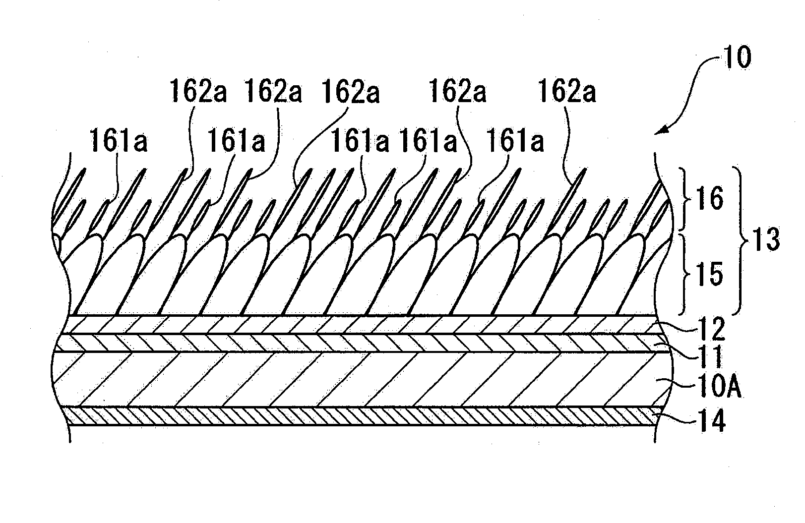
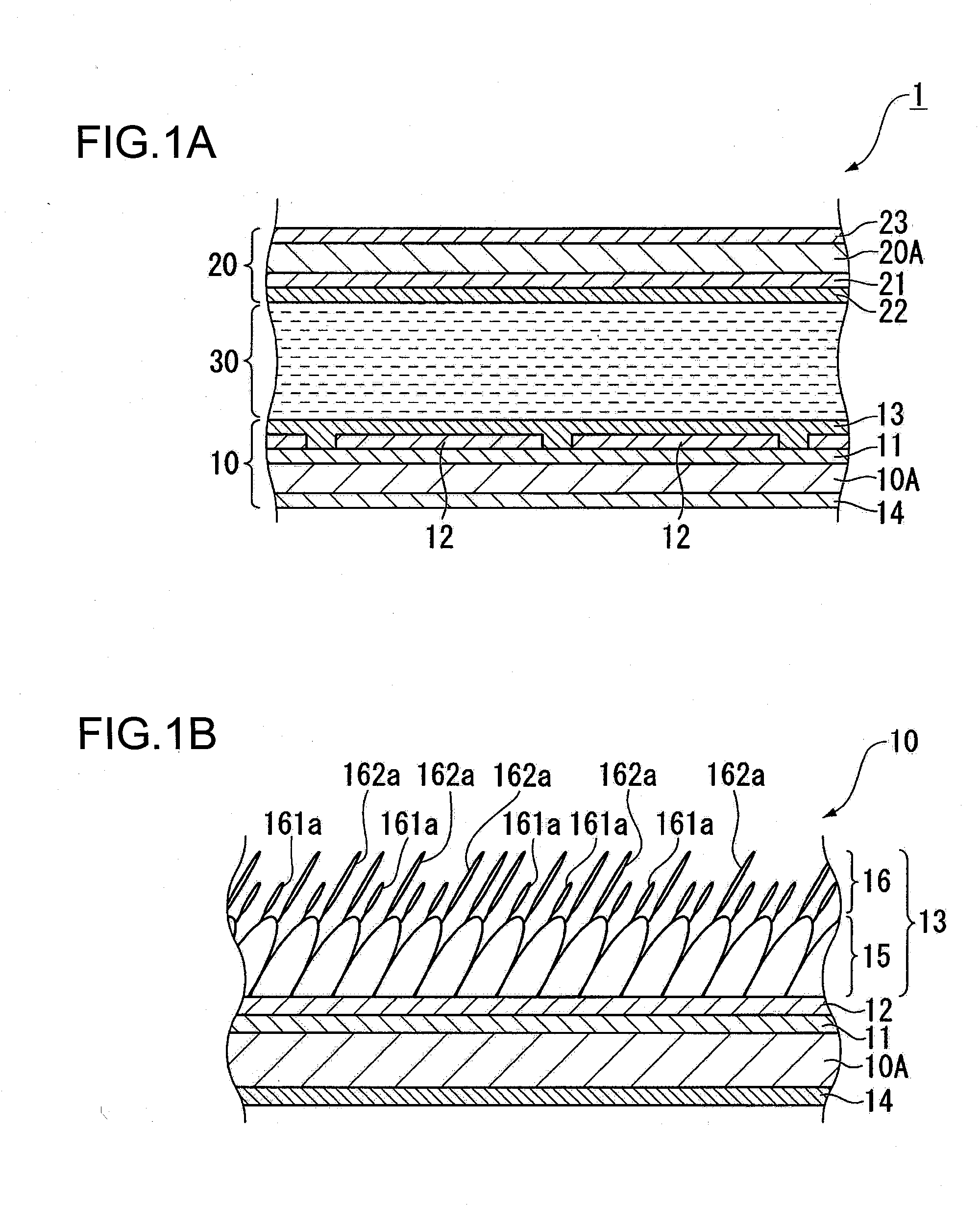
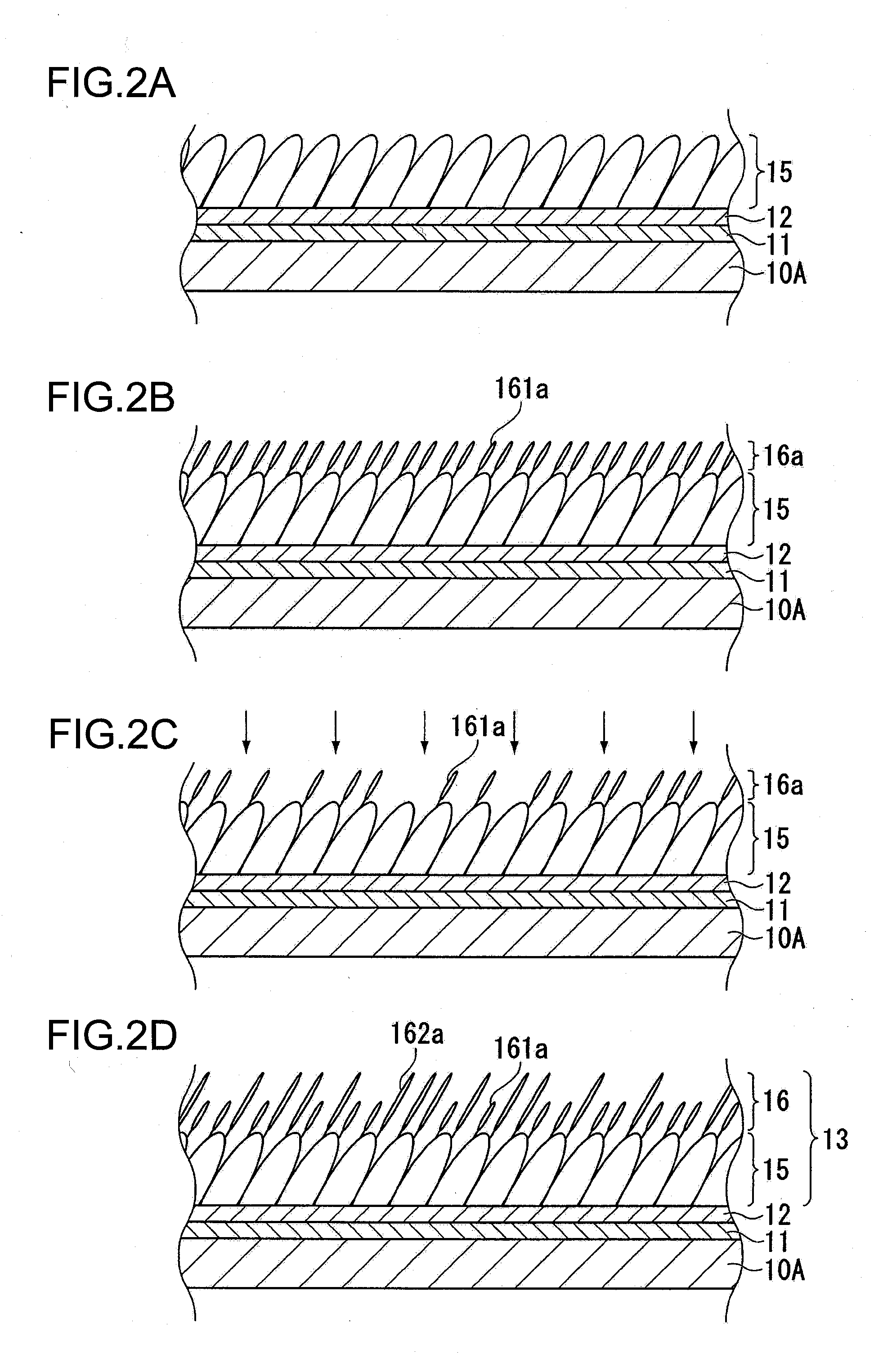
[0033]FIG. 1A is a cross-sectional view showing an example of the liquid crystal device manufactured using the invention, and FIG. 1B is a schematic diagram enlargedly showing an oriented film. As shown in FIG. 1A, the liquid crystal device 1 of the present embodiment is provided with an element substrate 10 (one substrate), an opposed sub...


PUM

PropertyMeasurementUnit
temperatureaaaaaaaaaa
wavelengthaaaaaaaaaa
timeaaaaaaaaaa

Abstract

A method of manufacturing a liquid crystal device provided with a liquid crystal layer held between a pair of substrates opposed to each other, and an oriented film disposed between at least one of the substrates and the liquid crystal layer, includes: (a) providing an inorganic oriented film to the one of the substrates; (b) forming a first organic film with a first silane-coupling agent, the first organic film randomly covering a surface of the inorganic oriented film with a predetermined coverage factor smaller than 1; and (c) forming, after step (b), a second organic film with a second silane-coupling agent having a carbon number different from a carbon number of the first silane-coupling agent, the second organic film covering the surface exposed from the first organic film, thereby forming the oriented film composed mainly of the first organic film, the second organic film, and the inorganic film.

Description

[0001]The entire disclosure of Japanese Patent Application No. 2008-180393, filed Jul. 10, 2008 is expressly incorporated by reference herein.BACKGROUND[0002]1. Technical Field[0003]The present invention relates to a method of manufacturing a liquid crystal device.[0004]2. Related Art[0005]Since the past, liquid crystal devices have widely been used as display sections of personal computers, cellular phones, and so on, or light valves or the like of projectors. The liquid crystal device is provided with, for example, a liquid crystal layer held between a pixel electrode and a common electrode, an oriented film for controlling the orientation of the liquid crystal molecules of the liquid crystal layer, and so on. When an electrical field is applied to the liquid crystal layer, the direction angles of the liquid crystal molecules vary, and the polarization state of the light passing through the liquid crystal layer is changed. Thus, a part of the light having passed through the liquid...

Claims


Application Information

Patent Timeline
Patent Type & Authority Applications(United States)
IPC IPC(8): B29D11/00B05D5/12
CPCY10T428/1005G02F1/133719C09K2323/02
Inventor ASUKE, SHINTARO
Owner SEIKO EPSON CORP
Why Eureka
Try Eureka