

Apparatus for manufacturing semiconductor
- Summary
- Abstract
- Description
- Claims
- Application Information
AI Technical Summary
Benefits of technology
Problems solved by technology
Method used
Image

Examples
first embodiment
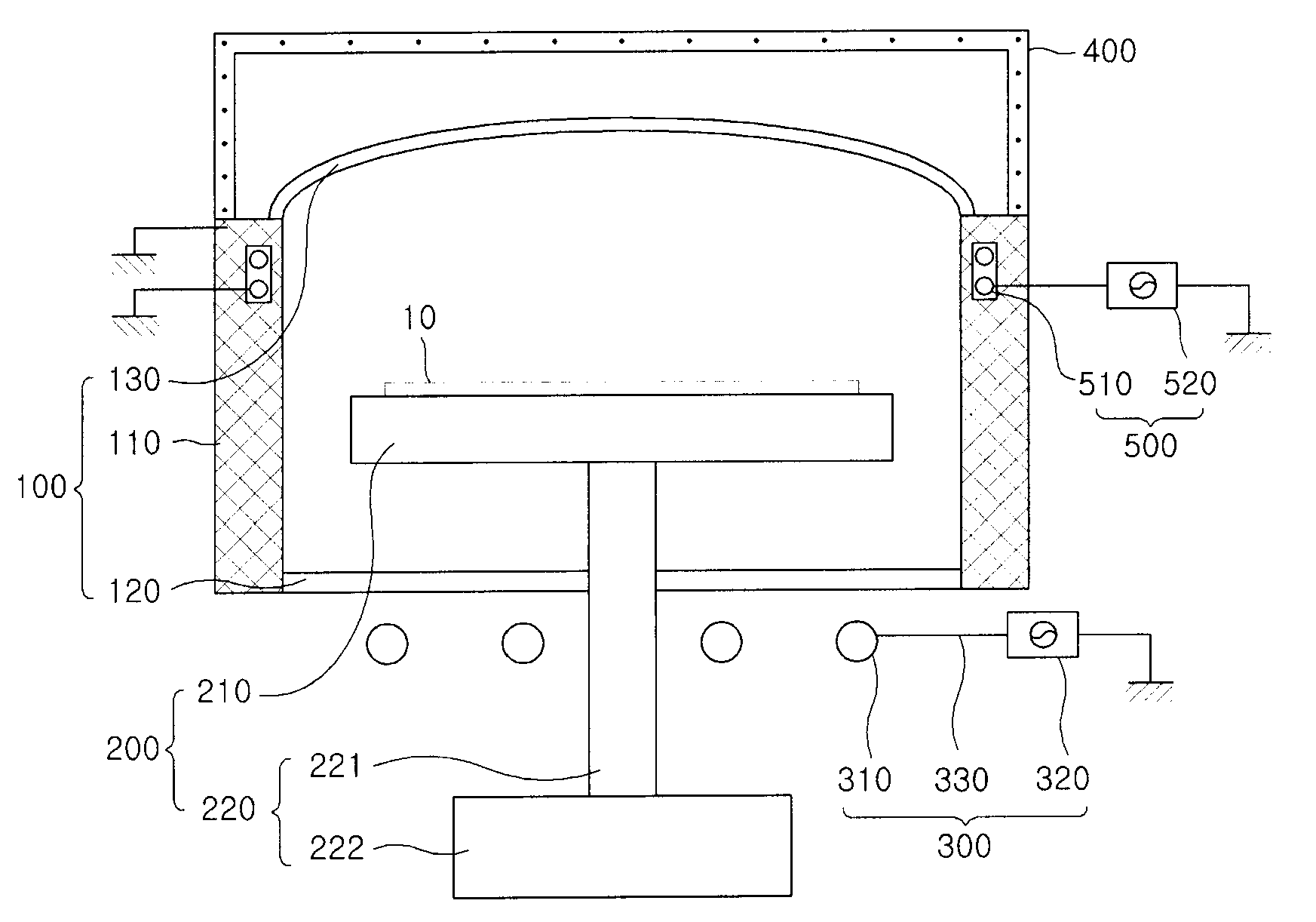
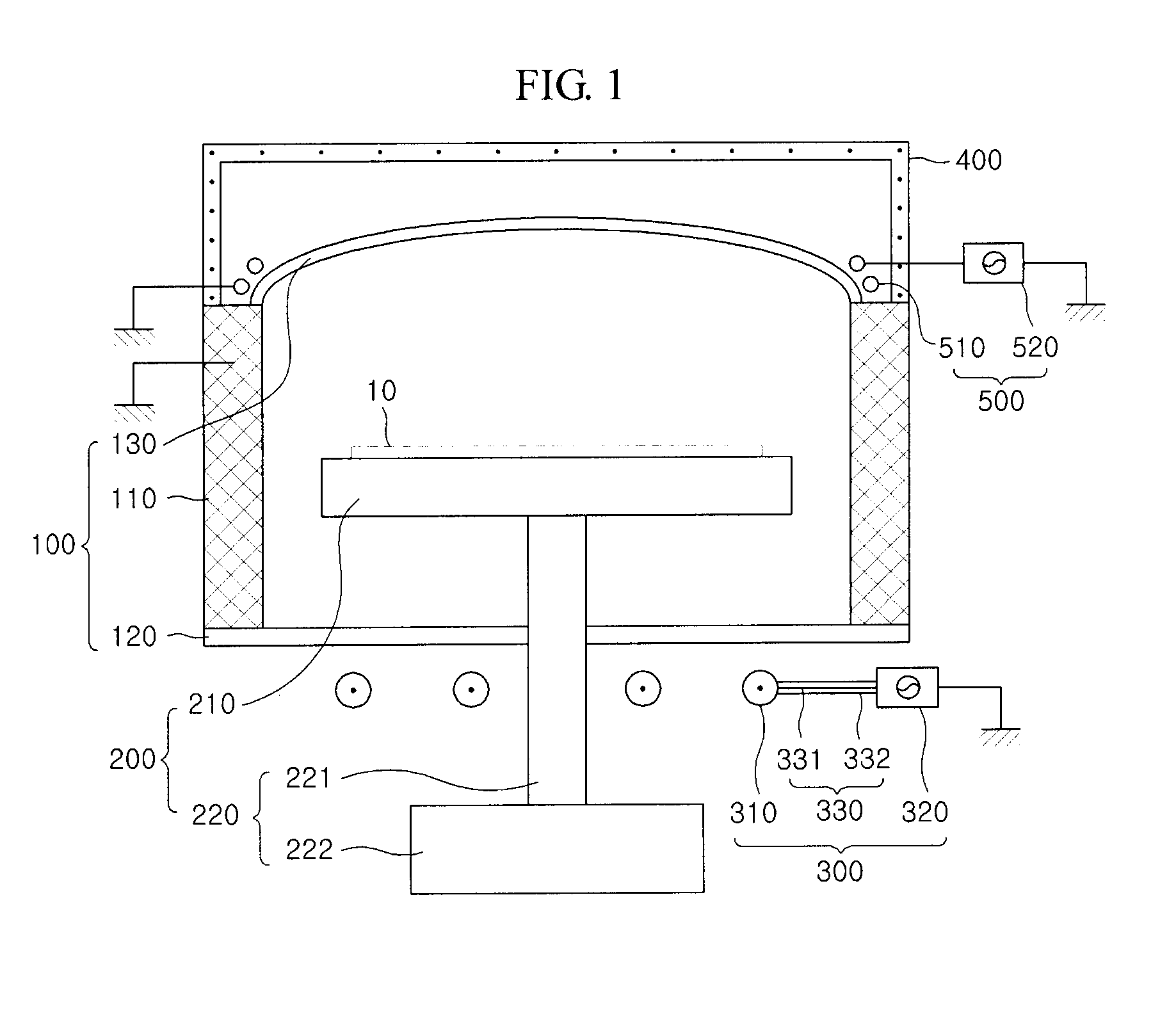
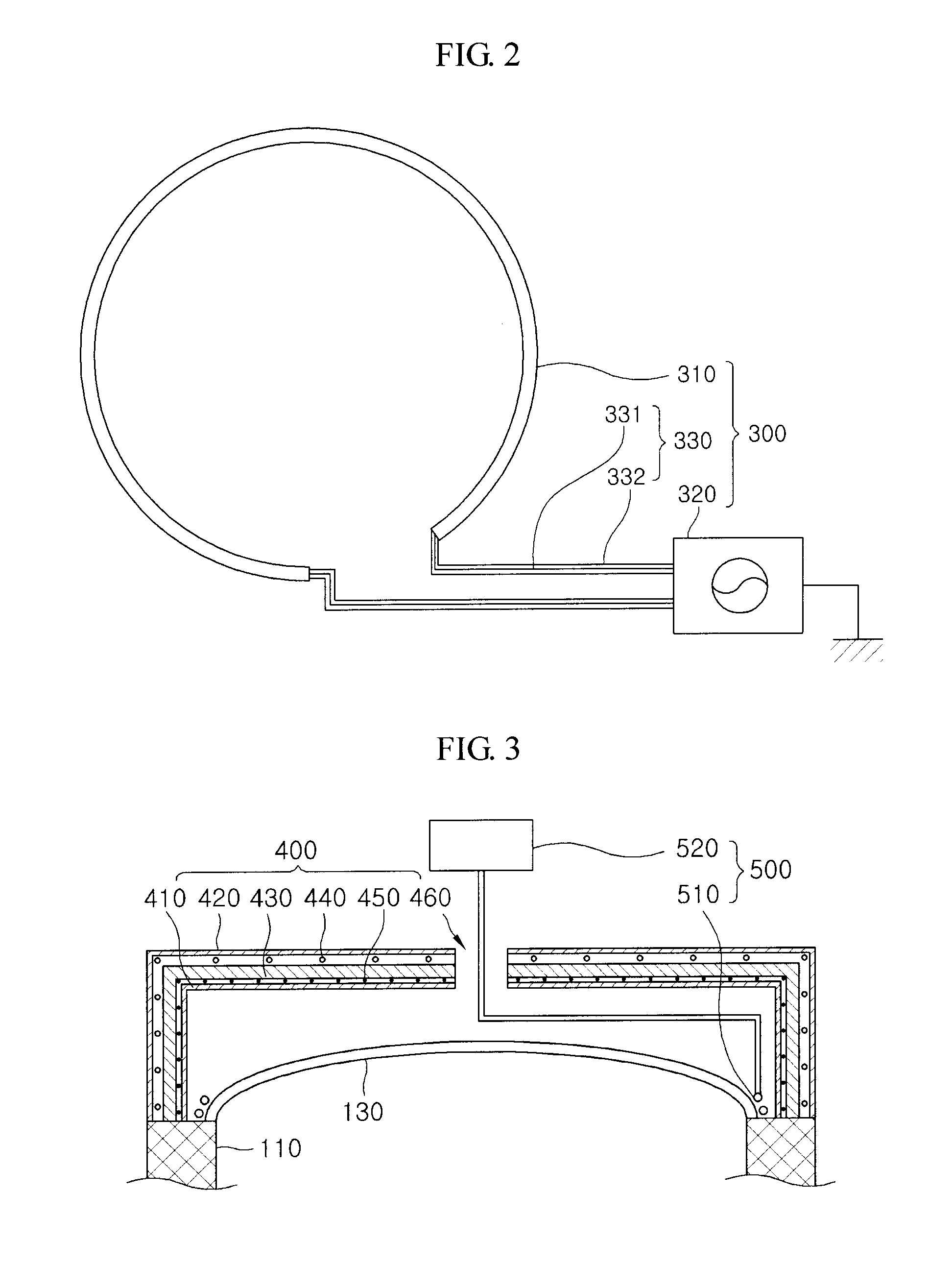
[0031]Referring to FIGS. 1 to 3, the semiconductor device manufacturing apparatus in accordance with the present invention includes a chamber 100 having a reaction space therein, a substrate disposing unit 200 to dispose a substrate 10 in the chamber 100, a first heating unit 300 disposed under the chamber 100 to heat the reaction space, a second heating unit 400 disposed over the chamber 100 to heat the reaction space, and a plasma generating unit 500 to generate plasma in the reaction space.
[0032]The chamber 100 includes a chamber body 110 forming an inner space, a base plate 120 and a top plate 130.
[0033]The chamber body 110 is fabricated in a cylindrical shape, but it is not limited thereto. The chamber body 110 may be formed in a polygonal shape. A portion or all of the chamber body 110 is preferably formed of a metallic material. In this embodiment, the chamber body 110 is formed using a material such as aluminum or stainless steel. Herein, the chamber body 110 acts as sidewal...
second embodiment
[0079]FIG. 7 illustrates a cross-sectional view of a semiconductor device manufacturing apparatus in accordance with the present invention.
[0080]Referring to FIG. 7, the semiconductor device manufacturing apparatus includes a chamber 100, a substrate disposing unit 200, a first heating unit 300 and a plasma generating unit 500. That is, this embodiment does not include a second heating unit 300.
[0081]It is effective to use a top plate 130 of the chamber 100 that is formed with a light non-penetrating material and includes a reflective film coated on its inner surface. As a result, radiant heat of the first heating unit 300 can be reflected by the reflective film and thus transmitted again to a reaction space of the chamber 100 without being emitted to the outside through the top plate 130. The top plate 130 and a base plate 120 of the chamber 100 may be formed in a domy shape to enhance heat balance.
[0082]An antenna 510 of the plasma generating unit 500 is disposed near an edge regi...
third embodiment
[0084]FIG. 8 illustrates a cross-sectional view of a semiconductor device manufacturing apparatus in accordance with the present invention.
[0085]Referring to FIG. 8, the semiconductor device manufacturing apparatus includes a chamber 100, a substrate disposing unit 200, a first and a second heating unit 300 and 400 and a plasma generating unit 500 including an antenna 510 disposed within the chamber 100.
[0086]The plasma generating unit 500 includes the antenna 510 disposed within a chamber body 110 of the chamber 100 and a high frequency power sector 520 connected to the antenna 510 to supply high frequency power to the antenna 510.
[0087]The chamber body 110 includes a hollow inner space at its upper portion. The hollow space is formed to have a circular band shape along a circumference of the chamber body 110, but it is not limited thereto. A portion of the chamber body 110 may be formed as a concave groove caving in from the outside to the inside. The antenna 510 is disposed in th...
PUM
| Property | Measurement | Unit |
|---|---|---|
| Temperature | aaaaa | aaaaa |
| Temperature | aaaaa | aaaaa |
| Temperature | aaaaa | aaaaa |
Abstract
Description
Claims
Application Information