

Soldering method and soldering apparatus
a soldering apparatus and soldering method technology, applied in the direction of soldering apparatus, final product manufacture,auxillary welding devices, etc., can solve the problems of inability to always use the method and the indirect application of ultrasonic oscillation through the circuit substrate, and achieve the effect of increasing the surface tension
- Summary
- Abstract
- Description
- Claims
- Application Information
AI Technical Summary
Benefits of technology
Problems solved by technology
Method used
Image

Examples
first embodiment
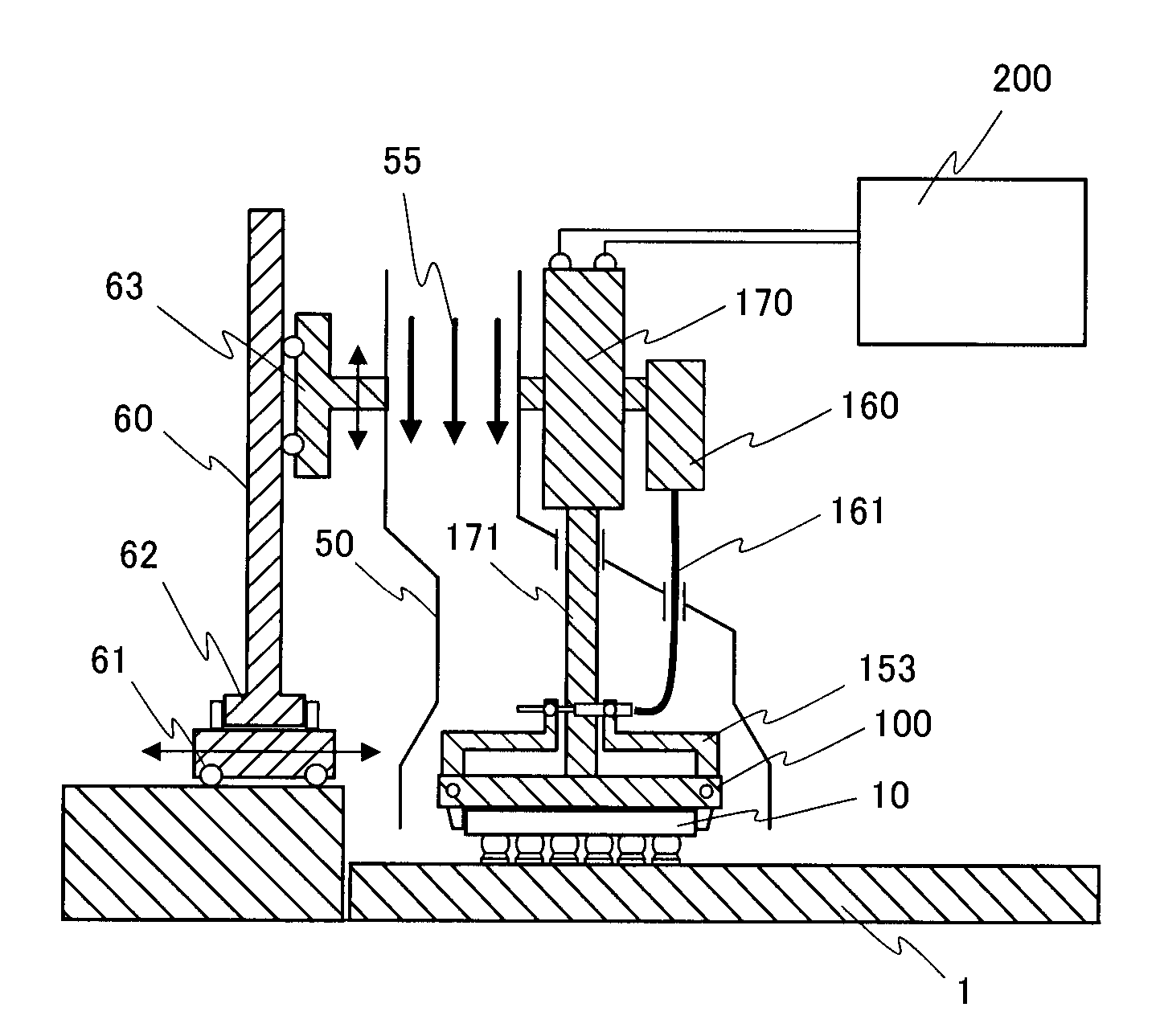
[0057]As a repair apparatus for a miniaturized bump connection component such as a BGA, there was used one that directly applied an output of 100 W of ultrasonic oscillation after the target component was connected to the transducer with the clamp during melting of the solder, and a BGA with full-grid 256 bumps of 1.27 mm-pitch 4-column peripheral arrangement which was poorly connected was removed.
[0058]The BGA was connected by pasting a solder whose composition was the same as that of bumps of an Sn—9Zn solder, so that another BGA which was to be newly exchanged was provided with the bumps of the same Sn—9Zn solder and the BGA was connected again by pasting the Sn—9Zn solder.
[0059]At the time of reconnecting the BGA, the solder bumps and the solder paste were melted 30 seconds later after heating, and 20 seconds later thereafter, cooling of the connection portion by stopping the supply of the hot air and the ultrasonic oscillation for 10 seconds were started. The ultrasonic oscilla...
second embodiment
[0065]As a local reflow apparatus for a surface connection component such as a connector, there was used one that directly applied an output of 100 W of ultrasonic oscillation after the electric component was connected to the transducer with the clamp during melting of the solder, and a connector with 0.5 mm-pitch 50-leads was connected to a thin circuit substrate with a thickness of 0.8 mm by pasting an Sn—3Ag—0.5Cu solder.
[0066]At the time of connection, the solder paste was melted 25 seconds later after heating, and 20 seconds later thereafter, cooling of the connection portion by stopping the supply of the hot air and the ultrasonic oscillation for 10 seconds were started.
[0067]The ultrasonic oscillation was applied to the connector with 0.5 mm-pitch 50-leads directly clamped through the transducer of the apparatus.
[0068]Further, the clamp was configured in such a manner that a portion to which the power (power level=about 15N) from the actuator that was provided with the contro...
third embodiment
[0072]As a repair apparatus for a miniaturized bump connection component such as a BGA, there was used one that directly applied an output of 100 W of ultrasonic oscillation after the target component was connected to the transducer with the clamp during melting of the solder, and a BGA with 1.0 mm-pitch full-grid 256 bumps which was poorly connected was removed.
[0073]The BGA was connected by pasting a solder whose composition was the same as that of bumps of an Sn—9Zn solder, so that another BGA which was to be newly mounted was provided with the bumps of the same Sn—9Zn solder and the BGA was connected again by pasting the Sn—9Zn solder.
[0074]At the time of reconnecting the BGA, the solder bumps and the solder paste were melted 30 seconds later after heating, and 20 seconds later thereafter, cooling of the connection portion by stopping the supply of the hot air and the ultrasonic oscillation for up to 20 seconds were started.
[0075]The ultrasonic oscillation was applied to the BGA...
PUM
| Property | Measurement | Unit |
|---|---|---|
| Force | aaaaa | aaaaa |
| Power | aaaaa | aaaaa |
| Energy | aaaaa | aaaaa |
Abstract
Description
Claims
Application Information