Image display device

a display device and image technology, applied in static indicating devices, instruments, electroluminescent light sources, etc., can solve the problem of not being able to properly set the gray level of the pixel circuit, and achieve the effect of avoiding an increase in crosstalk in the signal line and simple configuration

Active Publication Date: 2010-01-14
JOLED INC
View PDF2 Cites 3 Cited by
  • Summary
  • Abstract
  • Description
  • Claims
  • Application Information

AI Technical Summary

Benefits of technology

[0012]The light emission and non-light emission periods are initiated by controlling the write transistor and setting the light emission and non-light emission period start voltages, output to the signal line, to the terminal voltage of the holding capacitor. This permits sharing of control via the scan lines other than the write signal scan line among a plurality of lines. As a result, the write signal is set in such a manner as to sequentially delay the timings at which to set the light emission period start voltage between successive lines. Also, the power drive signal is commonly set in units of a plurality of successive lines. This provides simpler configuration for the each plurality of lines as a result of sharing of the power drive signal. Further, the drain voltage of the drive transistor is pulled up to high level using the power drive signal at a time other than when one of the terminals of the holding capacitor is connected to the signal line by the write signal in the pixel circuits in other lines. This avoids an increase in crosstalk in the signal line which would otherwise result from sharing of the power drive signal among a plurality of successive lines, making it possible to set the signal line potential to the terminal voltage of the holding capacitor. As a result, the gray level can be set properly for the pixel circuits even if pixel circuit control using the scan lines is shared among a plurality of lines.
[0013]The present invention permits proper setting of the gray level for the pixel circuits even if pixel circuit control using the scan lines is shared among a plurality of lines.

Problems solved by technology

As a result, it may be impossible to set the gray level properly for the pixel circuits.

Method used


Image

  • Image display device
  • Image display device
  • Image display device

Examples


embodiment 1

(1) Configuration of the Embodiment

(1-1) Overall Configuration

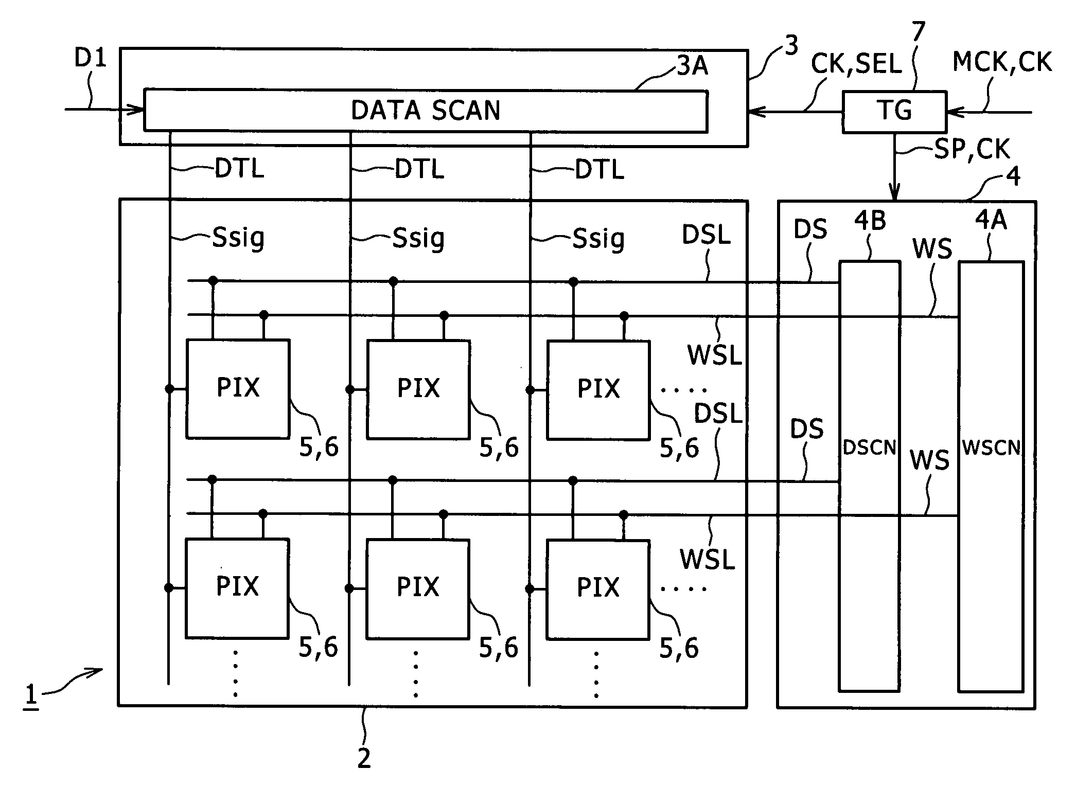
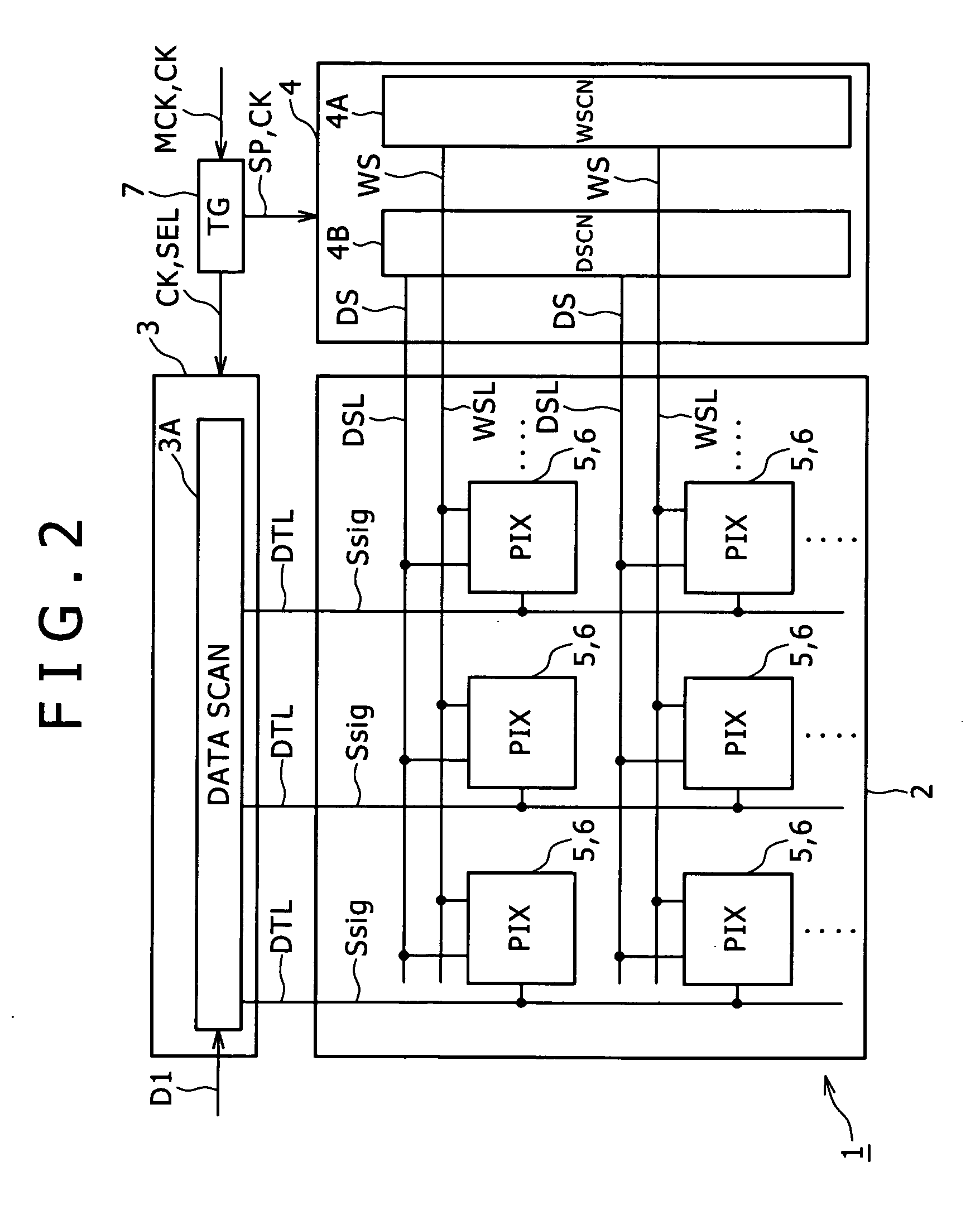
[0029]FIG. 2 is a block diagram illustrating an image display device according to this embodiment. An image display device 1 has a display section 2 formed on an insulating substrate made, for example, of glass. In the image display device 1, a signal line drive circuit 3 and scan line drive circuit 4 are formed around the display section 2.

[0030]The display section 2 has pixel circuits 5 arranged in a matrix form. Each of the pixel circuits 5 includes a pixel (PIX) 6. A timing generator (TG) 7 receives a master clock MCK, clock CK and other signals. The master clock MCK is synchronous with a vertical synchronizing signal. The clock CK is synchronous with image data D1. The timing generator 7 processes these signals and outputs a predetermined sampling pulse SP, the clock CK, a selector control signal SEL and other signals.

[0031]The scan line drive circuit 4 outputs a write signal WS and power drive signal DS respectively...

embodiment 2

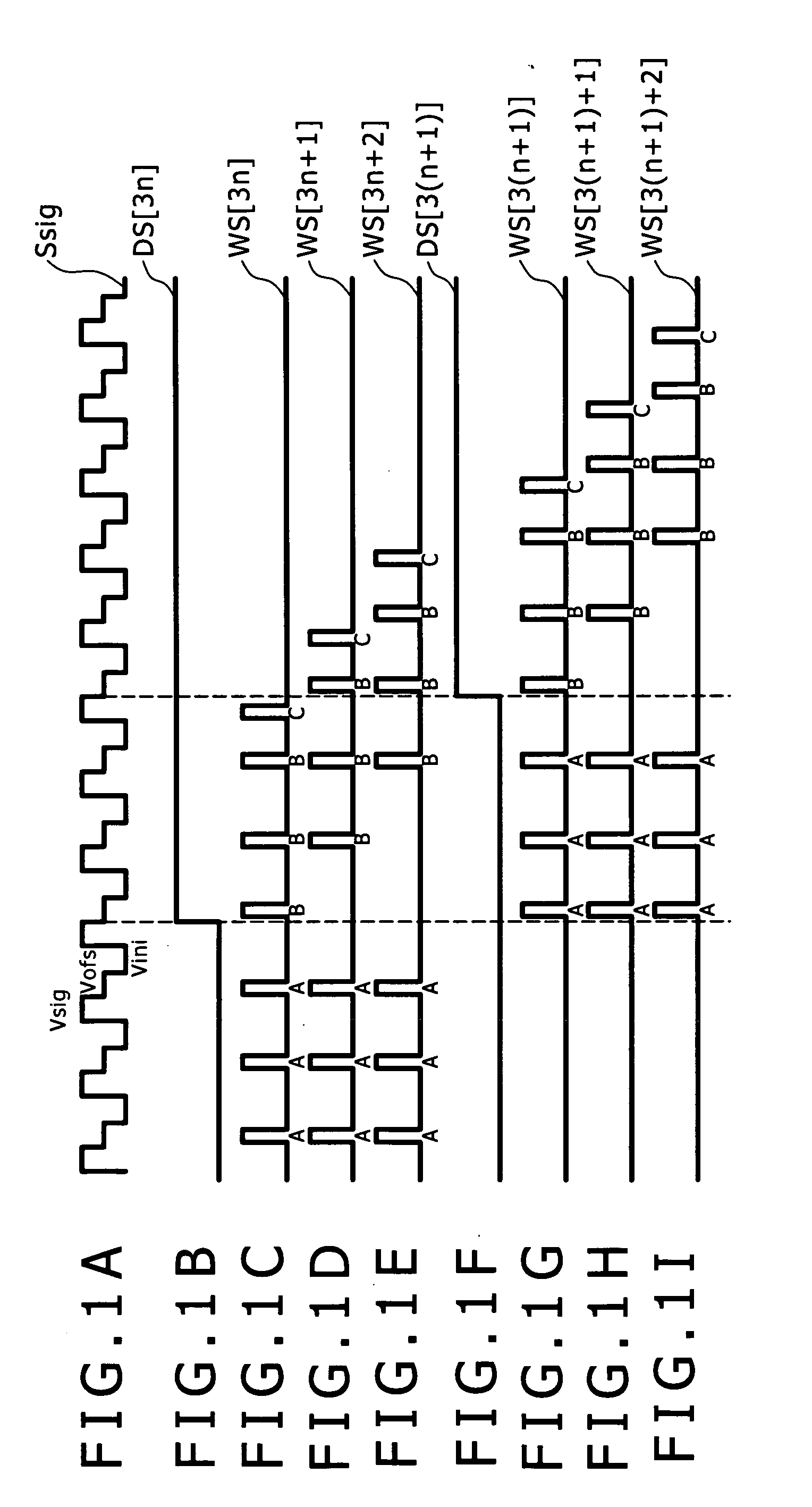
[0088]FIGS. 13A to 13G are timing diagrams for describing, in comparison with FIG. 1, the operation of an image display device according to embodiment 2 of the present invention. The image display device according to the present embodiment generates the drive signal Ssig of the signal line DTL in such a manner that the same signal Ssig changes in voltage level in order of the extinguishing fixed voltage Vini, fixed voltage Vofs for threshold voltage variation correction and gray level setting voltage Vsig. This provides a greater difference in signal level when the drive signal Ssig is pulled down to low level than in embodiment 1.

[0089]The image display device according to the present embodiment generates the write signals WS and drive signal DS according to the setting of the drive signal Ssig of the signal line DTL. The image display device according to the present embodiment is configured in the same manner as that according to embodiment 1 except for the above difference relati...

embodiment 3

[0091]FIGS. 14A to 14G are timing diagrams for describing, in comparison with FIGS. 13A to 13G, the operation of an image display device according to embodiment 3 of the present invention. As with the display device according to embodiment 2, the image display device according to the present embodiment generates the drive signal Ssig of the signal line DTL in such a manner that the same signal Ssig changes in voltage level in order of the fixed voltage Vini, fixed voltage Vofs and gray level setting voltage Vsig. The image display device shown in FIGS. 14A to 14G has the pixel circuits 5 grouped in units of five lines.

[0092]The image display device according to the present embodiment generates the write signals WS and drive signal DS according to the setting of the drive signal Ssig of the signal line DTL. The image display device according to the present embodiment is configured in the same manner as that according to embodiment 2 except for the above difference relating to the sig...


PUM


Abstract

Disclosed herein is an image display device including a display section formed by arranging pixel circuits in a matrix form. Each pixel circuit includes at least a light emitting element, a drive transistor, a holding capacitor, and a write transistor. A light emission and non-light emission periods are alternately repeated. A light emission period start voltage and a non-light emission period start voltage are alternately output to the signal line. The terminal voltage of the holding capacitor is set to start the light emission and non-light emission periods. The write signal is set to sequentially delay the timings. The power drive signal is set in units of a plurality of successive lines. The drain voltage of the drive transistor is pulled up to high level at a time other than when the one of the terminals is connected to the signal line by the write signal in different lines.

Description

BACKGROUND OF THE INVENTION[0001]1. Field of the Invention[0002]The present invention relates to an image display device and is applicable, for example, to an active matrix image display device using organic EL (Electro Luminescence) elements. The present invention pulls a power drive signal up to high level at a time other than when a write signal is high. This permits the gray level to be set properly for each pixel circuit even if pixel circuit control using scan lines is shared among a plurality of lines.[0003]2. Description of the Related Art[0004]Recent years have seen the brisk development of active matrix image display devices using organic EL elements as their light-emitting elements. Here, the term “active matrix image display devices using organic EL elements” refer to image display devices which rely on light emission from an organic thin film when the film is applied with an electric field. These elements can be driven by a small voltage of 10 V or less, providing reduc...

Claims


Application Information

Patent Timeline
Patent Type & Authority Applications(United States)
IPC IPC(8): G09G3/20H05B44/00
CPCG09G3/3266G09G2320/043G09G2310/06G09G2300/0861
Inventor HANDA, TOMOAKIUCHINO, KATSUHIDEYAMAMOTO, TETSURO
Owner JOLED INC
Why Eureka
Try Eureka