Semiconductor ceramic composition and process for producing the same

a technology of semiconductor ceramics and compositions, applied in the direction of electrical equipment, inorganic chemistry, conductive materials, etc., can solve the problems of inability to obtain desired characteristics and incomplete solid solutions, and achieve the effect of enhancing the sinterability of the composition and ensuring the resistivity of the composition

Inactive Publication Date: 2010-01-21
HITACHI METALS LTD
View PDF9 Cites 9 Cited by
  • Summary
  • Abstract
  • Description
  • Claims
  • Application Information

AI Technical Summary

Benefits of technology

[0034]In the steps of preparing the above-mentioned calcined powders, the starting material powders may be crushed in mixing depending upon the grain sizes of the material powders. Mixture and crushing may be performed by any of wet mixing and crushing using pure water and ethanol, and dry mixing and crushing, but dry mixing and crushing is preferred for the reason of capable of restraining compositional deviation. Further, BaCO3, Na2CO3 and TiO2 are exemplified as the starting materials in the above, but the advantage of the invention is not impaired even when other Ba compounds, Na compounds and the like are used.
[0035]As described above, after separately preparing a Ba(TiM)O3 calcined powder and a (BiNa)TiO3 calcined powder, the calcined powders are mixed each in a prescribed amount. Mixing may be performed by any of wet mixing using pure water and ethanol, and dry mixing, but dry mixing is preferred for capable of restraining compositional deviation. Depending upon the grain sizes of the calcined powders, crushing may be carried out after mixing, or mixing and crushing may be performed at the same time. The average grain size of the mixed calcined powder after mixing and crushing is preferably from 0.6 to 1.5 μm.
[0036]In the above-mentioned step of preparing the Ba(TiM)O3 calcined powder and / or the step of preparing the (BiNa)TiO3 calcined powder, or in the step of mixing the calcined powders, adding at most 3.0 mol % of Si oxide and at most 4.0 mol % of Ca oxide or Ca carbonate is favorable because Si oxide may restrain the abnormal growth of crystal grains and may readily control the resistivity of the composition, and Ca oxide or Ca carbonate may enhance the sinterability of the composition at low temperatures and may control the reducibility thereof. However, when either one of them is added in an amount exceeding the above-mentioned limit, then it is unfavorable since the composition cannot be semiconductive. Preferably, the addition is attained before mixing in each step.
[0037]A semiconductor ceramic composition according to the invention can be obtained by forming and sintering the mixed calcined powder obtained in the step of mixing the Ba(TiM)O3 calcined powder and the (BiNa)TiO3 calcined powder. One example of a process after the step of mixing the calcined powders is described below, to which, however, the invention should not be limited. Any and every known method is employable in the invention.
[0038]The mixed calcined powder obtained in the step of mixing a Ba(TiM)O3 calcined powder and a (BiNa)TiO3 calcined powder may be formed by any desired forming means. Before forming, if desired, the crushed powder may be granulated in a granulation apparatus. The density of the compact after the forming is preferably from 2 to 3 g / cm3.
[0039]The sintering may be attained in air or in a reducing atmosphere, or in an inert gas atmosphere having a low oxygen concentration, at a sintering temperature of from 1200° C. to 1400° C. for a sintering time of from 2 hours to 6 hours. One preferred embodiment of the sintering step is described below. In case where the powder is granulated before forming, it is preferably processed for binder removal at 300° C. to 700° C. before sintering.

Problems solved by technology

However, although the evaporation of Bi is certainly restrained by this method, a complete solid solution cannot be formed and the desired characteristics cannot be obtained.

Method used


Image

  • Semiconductor ceramic composition and process for producing the same

Examples


example 1

[0052]BaCO3 and TiO2 as main materials and Nb2O5 as a semiconductor ingredient powder were prepared and blended so as to be Ba(Ti0.998Nb0.002)O3, followed by mixing in pure water. The obtained mixed material powder was calcined at 1000° C. for 4 hours to prepare a Ba(TiNb)O3 calcined powder.

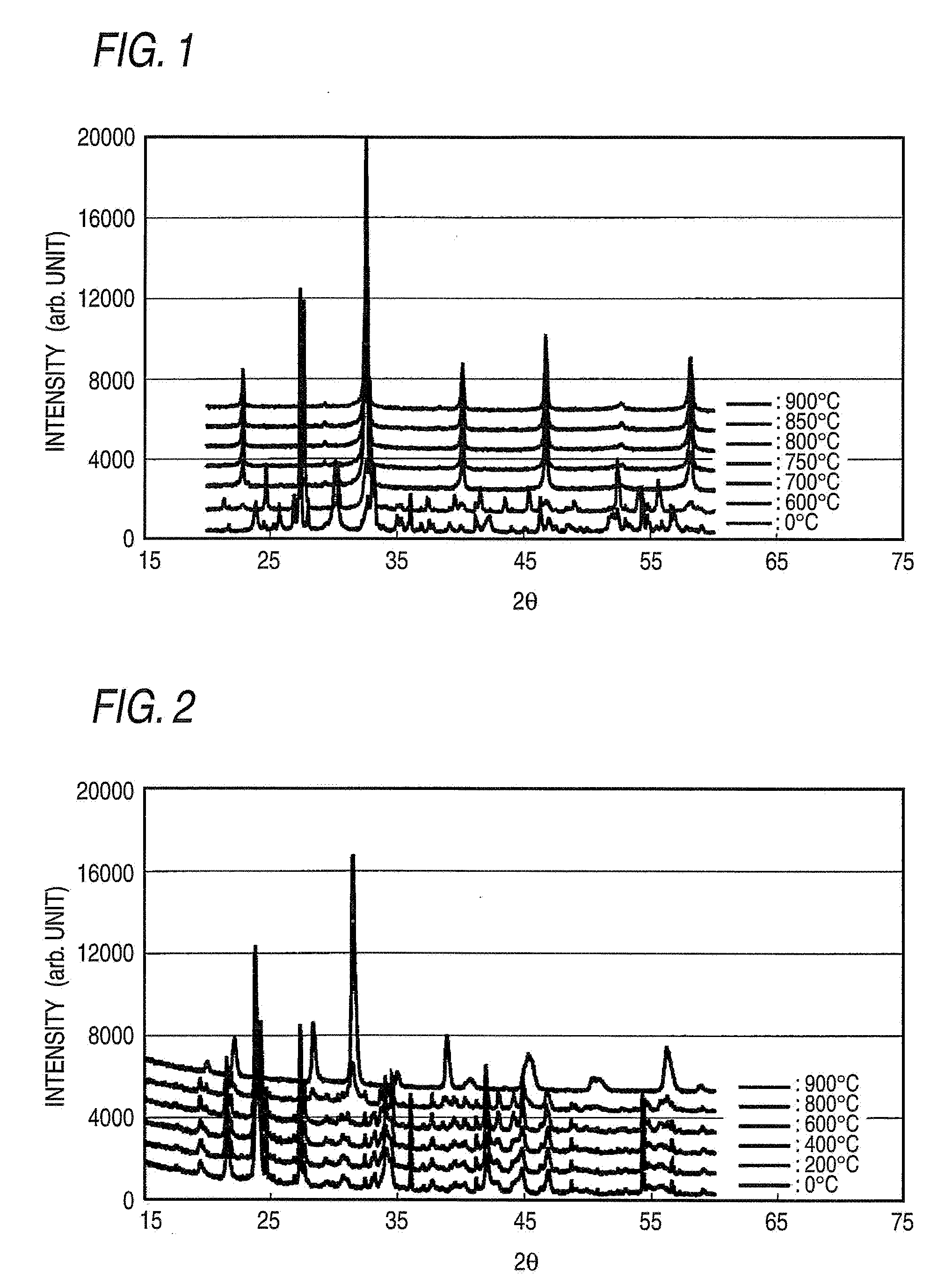
[0053]Na2CO3, Bi2O3 and TiO2 as material powders were prepared and blended so as to be (Bi0.5Na0.5)TiO3, followed by mixing in ethanol. The obtained mixed material powder was calcined in air at 600° C. to 900° C. for 4 hours to prepare a (BiNa)TiO3 calcined powder. FIG. 1 shows the X-ray diffraction patterns of the obtained (Bi0.5Na0.5)TiO3 calcined powder at different calcination temperatures of from 600° C. to 900° C.

[0054]The Ba(TiNb)O3 calcined powder and the (BiNa)TiO3 calcined powder calcined at 800° C. were blended so as to be 73 / 7 in a molar ratio, then 0.4 mol % of SiO2 and 1.4 mol % of CaCO3 were added thereto as sintering promoters, and these were mixed and crushed in a pot mill with p...


PUM

PropertyMeasurementUnit
temperatureaaaaaaaaaa
Curie temperatureaaaaaaaaaa

Abstract

It is intended to provide a semiconductor ceramic composition in which a part of Ba in BaTiO3 is substituted with Bi—Na, which is capable of restraining the evaporation of Bi in the calcination step, is capable of restraining the compositional deviation of Bi—Na thereby suppressing the formation of different phases, is capable of further reducing the resistivity at room temperature, and is capable of restraining the fluctuation of the Curie temperature; and to provide a production process of the same. When a calcined Ba(TiM)O3 powder (M is a semiconductor dopant) and a calcined (BaNa)TiO3 powder are separately prepared and the Ba(TiM)O3 powder is calcined at a relatively high temperature while the (BaNa)TiO3 powder is at a relatively low temperature, both at the most suitable temperatures for them, then the evaporation of Bi may be retarded and the compositional deviation of Bi—Na may be thereby suppressed to inhibit the formation of different phases; and when these calcined powders are mixed, formed and sintered, then a semiconductor ceramic composition which has a low resistivity at room temperature and is capable of restraining the fluctuation of the Curie temperature can be obtained.

Description

CROSS-REFERENCE TO RELATED APPLICATIONS[0001]This application claims the benefit of PCT International Patent Application No. PCT / JP2007 / 070958, filed Oct. 26, 2007, and Japanese Patent Application No. 2006-298304, filed Nov. 1, 2006, in the Japanese Patent Office, the disclosures of which are incorporated herein by reference.BACKGROUND OF THE INVENTION[0002]1. Field of the Invention[0003]The present invention relates to a semiconductor ceramic composition having a positive resistive temperature, which is used for a PTC thermistor, a PTC heater, a PTC switch, a temperature detector and the like, and a process for producing the same.[0004]2. Description of the Related Art[0005]As materials showing a PTCR characteristic (Positive Temperature Coefficient of Resistivity), compositions in which various semiconductor dopants are added to BaTiO3 have been conventionally proposed. These compositions have a Curie temperature around 120° C. Depending upon the use, it becomes necessary for thes...

Claims


Application Information

Patent Timeline
Patent Type & Authority Applications(United States)
IPC IPC(8): H01B1/08
CPCC04B35/4682H01C17/06533C04B35/62685C04B2235/3201C04B2235/3208C04B2235/3234C04B2235/3251C04B2235/3294C04B2235/3298C04B2235/3418C04B2235/5436C04B2235/6562C04B2235/6565C04B2235/6584H01C7/025C04B35/62675C04B35/46H01C7/02
Inventor SHIMADA, TAKESHITOJI, KAZUYA
Owner HITACHI METALS LTD
Why Eureka
Try Eureka