Switching power supply device and method for adjusting dead time thereof
- Summary
- Abstract
- Description
- Claims
- Application Information
AI Technical Summary
Benefits of technology
Problems solved by technology
Method used
Image

Examples
first embodiment
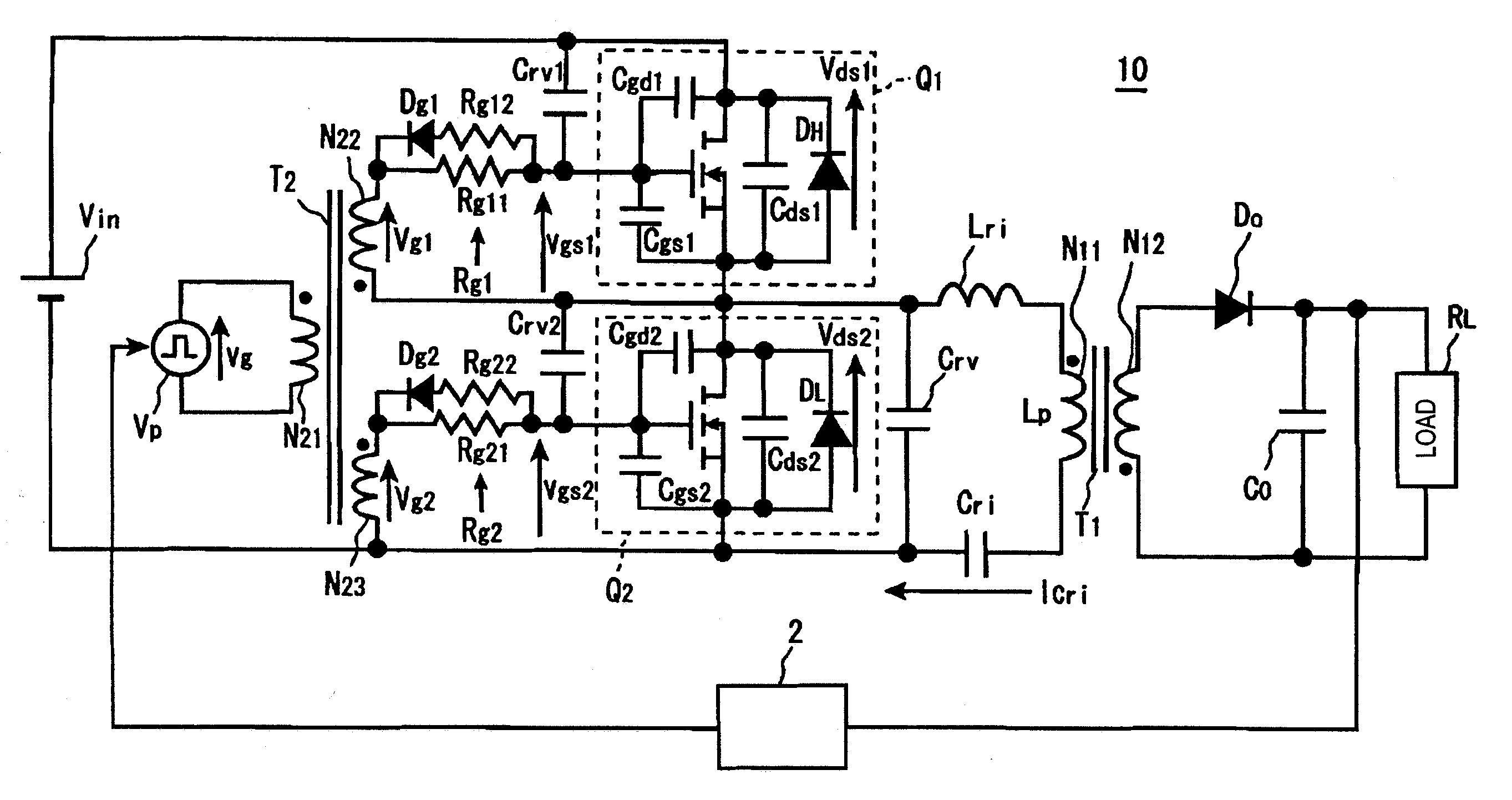
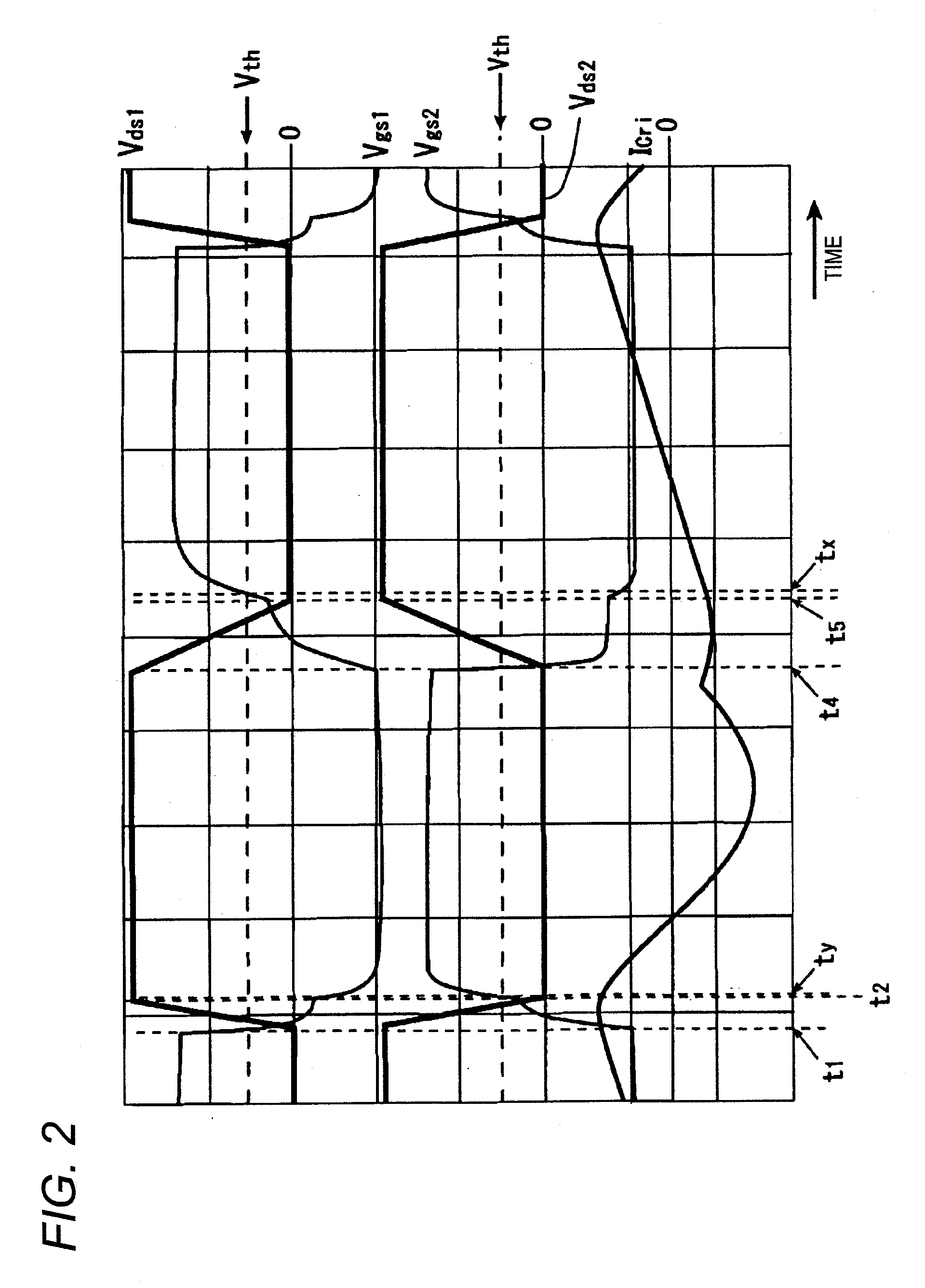
[0059]FIG. 1 shows a circuit configuration of the switching power supply device according to a first embodiment of the present invention. In this embodiment, and N channel MOSFET is used in each of a high side switching element Q1 and a low side switching element Q2. In the switching power supply device 10, gate signals of the switching element Q I and the switching element Q2 are generated from one gate signal Vg by a secondary winding N22 and a tertiary winding N23 of one (single) drive transformer T2 as gate signals Vg1 and Vg2 which are mutually reversed. Further, capacitors Crv1 and Crv2 are connected in parallel respectively to parasitic capacitors Cgd1 and Cgd2 formed between the gate and the source of the respective switching elements Q1 and Q2, and values of the gate-drain capacitor and gate resistors are adjusted such that a voltage developed on the gate resistors Rg1, Rg2 is increased by a resonant circulation current, thereby to make a gate voltage lower than an ON thres...
second embodiment
[0079]FIG. 4 shows a circuit configuration of a switching power supply device 20 according to a second embodiment of the present invention. The present embodiment provides a full-wave current resonance circuit which is different from the first embodiment in that the output transformer T1 of the first embodiment is changed to an output transformer T3 including a primary winding N31, a secondary winding N32 and a tertiary winding N33, and the rectifying smoothing circuit is changed to a full-wave rectification circuit. Other configurations are the same as those in the first embodiment. FIG. 5 shows operating waveforms. The individual waveforms shown in FIG. 5 are similar to those shown in FIG. 2. However, the output transformer T3 is provided with the secondary winding N32 and the tertiary winding N33, thereby giving a circuit which is symmetrical in polarity of the output voltage. Thus, the operations are reversed in polarity every half cycle of switching and substantially symmetrica...
third embodiment
[0080]FIG. 6 shows a circuit configuration of a switching power supply device 30 according to a third embodiment of the present invention. The present embodiment shows a case where a drive transformer T4 is used only on the high side. Although the drive transformer T4 is used on the high side in the present embodiment, the drive transformer may be used only on the low side. A rectifying smoothing circuit 3 is a simplified type of the rectifying smoothing circuit used in the first embodiment and the second embodiment. FIG. 7 shows operating waveforms when the switching power supply device 30 is changed to a half-wave current resonance circuit. The operations of the present embodiment are fundamentally similar to those of the first embodiment. In the present embodiment, a level shift (signal isolation) on the high side (or on the low side) can be conducted by the drive transformer T4. With the present embodiment, the same effect as that obtained in the first embodiment can be obtained...
PUM
 Abstract
Description
Claims
Application Information
 - R&D Engineer
- R&D Manager
- IP Professional
- Industry Leading Data Capabilities
- Powerful AI technology
- Patent DNA Extraction
Browse by: Latest US Patents, China's latest patents, Technical Efficacy Thesaurus, Application Domain, Technology Topic.
© 2024 PatSnap. All rights reserved.Legal|Privacy policy|Modern Slavery Act Transparency Statement|Sitemap