Semiconductor device

Inactive Publication Date: 2010-09-02
RENESAS ELECTRONICS CORP
View PDF3 Cites 43 Cited by
  • Summary
  • Abstract
  • Description
  • Claims
  • Application Information

AI Technical Summary

Benefits of technology

[0014]Writing to a memory array is enabled in the first operation mode and in the second operation mode. Therefore, when there is possibility of a write data correction, data is written in the first operation mode. When rewriting of data becomes unnecessary, the second operation mode is set and data is written. Accordingly, in a norma

Problems solved by technology

Therefore, when a PROM area is arranged near the MRAM cell array which stores the ordinary data and when data for setting various operating states (operating environment) is stored in the PROM area, disturbance occurs to the data of the PROM area due to a leakage magnetic field of a magnetic field induced at the time of writing of the ordinary data into the memory cell array.
Therefore, there arises a problem that the held data might be destroyed when influence of the leakage magnetic field is exerted over a long period of time.
Also in Patent Document 1, when data for operating characteristic adjustment and for operating environment setup of the flash memory cell array is stored in the OTP memory area

Method used


Image

  • Semiconductor device
  • Semiconductor device
  • Semiconductor device

Examples


Example

Embodiment 1

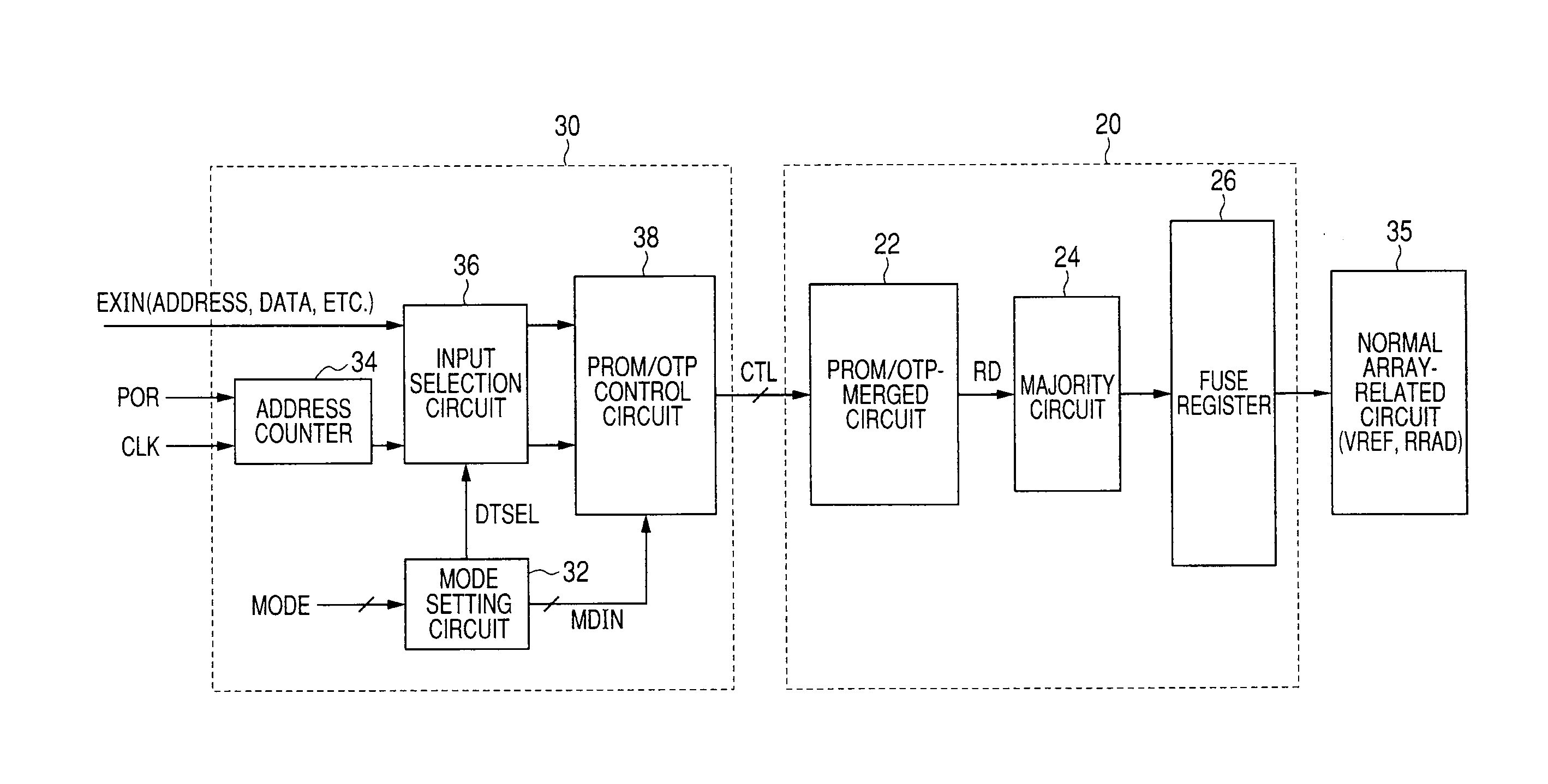
[0083]FIG. 1 illustrates roughly a chip layout of a nonvolatile memory unit of a semiconductor device according to the present invention. In FIG. 1, the nonvolatile memory unit of the semiconductor device is an MRAM including an MRAM cell which utilizes a variable magnetoresistive element as a data storage element.

[0084]In FIG. 1, a normal array 2 is arranged over a semiconductor chip region 1 in the shape of a rectangle. In the normal array 2, MRAM cells are arranged in a matrix and hold data which is accessible from the exterior. The present semiconductor chip region 1 may be a chip as a single body, or may be a macro area which is a part of area over a semiconductor chip and forms a part of a system LSI.

[0085]Adjoining to the normal array 2, a PROM / OTP-merged circuit block 4 and a main control circuit block 6 are arranged in a rectangle area, respectively. The PROM / OTP-merged circuit block 4 includes a common MRAM cell array and operates as either PROM or OTPROM (here...

Example

Embodiment 2

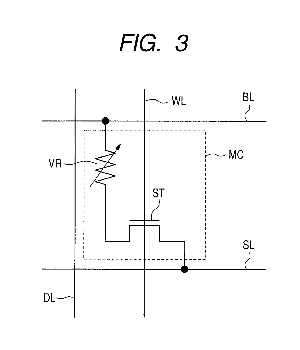
[0273]FIG. 30 is a drawing illustrating configuration of the principal part of a PROM / OTP-merged circuit according to Embodiment 2 of the present invention with cell structure of a normal array. In FIG. 30, a memory cell MC comprises a series body of a variable magnetoresistive element VR and a select transistor ST in a PROM / OTP array 40. The gate insulating film of the select transistor ST has a film thickness of Tox1.

[0274]On the other hand, in a bit-line write drive circuit 70, an OTP write drive circuit which performs data writing in an OTP mode is illustrated. In the OTP write drive circuit, a CMOS transmission gate 170 and a write column selection gate 172 are coupled in series between a bit line BL and a node which supplies a high bit-line writing voltage VREFBL. The CMOS transmission gate 170 includes a parallel body of a P-channel MOS transistor PT and an N-channel MOS transistor NT1, and write control signals TGEN_CEL and ZTGEN_CEL are supplied to the respectiv...

Example

Embodiment 3

[0393]FIG. 58 is a flow chart illustrating operation of a semiconductor device according to Embodiment 3 of the present invention. Hereafter, with reference to FIG. 58, operation of the semiconductor device according to Embodiment 3 of the present invention is explained.

[0394]After completion of manufacturing process of a semiconductor integrated circuit device, a wafer-level test is conducted (Step SS1). In the wafer-level test, a pad over a chip is exposed, and various characteristic tests are conducted by contacting a test probe to the pad. Detection of a bad cell of a memory cell, etc. are also performed by applying test data. In the first test, a test is carried out according to a default value of operating environment setup data.

[0395]In the test, test result data about each test item is collected (Step SS2). After the completion of the wafer-level test, it is determined whether a semiconductor device under test is a nondefective article which satisfies specificati...


PUM


Abstract

Data which sets up operation parameters, etc. of an internal circuit is supplied stably over a long period of time. In a cell array in which MRAM cells are arranged, read/write of test data is performed in a PROM mode. Finally, data writing is specifically performed to the memory cells in an OTP mode.

Description

CROSS REFERENCES TO RELATED APPLICATIONS[0001]The disclosure of Japanese Patent Application No. 2009-45815 filed on Feb. 27, 2009 and Japanese Patent Application No. 2009-208331 filed on Sep. 9, 2009 each including the specification, drawings and abstract are incorporated herein by reference in its entirety.BACKGROUND OF THE INVENTION[0002]The present invention relates to a semiconductor device, in particular, to configuration of a storage unit which stores internal operation environment setup data, such as trimming data and repair data, in a nonvolatile manner. More specifically, the present invention relates to a magnetic semiconductor memory unit in the semiconductor device which utilizes a variable magnetoresistive element as a data storage element.[0003]One of the nonvolatile semiconductor memories which store data in a nonvolatile manner includes a magnetic semiconductor memory (MRAM). The MRAM utilizes a variable magnetoresistive element, such as an MTJ element (magnetic tunn...

Claims


Application Information

Patent Timeline
IPC IPC(8): G11C11/00G11C7/00
CPCG11C7/20G11C8/08G11C11/16G11C17/14G11C17/146H01L27/228G11C29/023G11C29/028G11C2029/1204G11C2029/4402G11C29/021H10B61/22
Inventor OKAYAMA, SHOTA
Owner RENESAS ELECTRONICS CORP
Why Eureka
Try Eureka