Semiconductor light emitting device and method for manufacturing the same

a technology of semiconductors and light emitting devices, which is applied in the direction of semiconductor/solid-state device manufacturing, semiconductor devices, electrical devices, etc., can solve the problems of difficulty in taking out light, and finally lowering external quantum efficiency, so as to improve the efficiency of taking out light, reduce the effect of total reflection and easy attenuation

Active Publication Date: 2010-01-28
ROHM CO LTD
View PDF4 Cites 8 Cited by
  • Summary
  • Abstract
  • Description
  • Claims
  • Application Information

AI Technical Summary

Benefits of technology

[0015]Since nitride semiconductor is very hard material which is hardly etched by a wet etching process, chips can not be separated by dicing including etching for strain relaxation, in a light emitting device using nitride semiconductor. Therefore, the separation of chips is carried out by dicing or scribing a substrate after forming separation grooves at a region to be separated of the semiconductor lamination portion by a dry etching process. In the present invention, since a separation groove region is etched such that a perfect groove is not formed but parts of the semiconductor lamination portion of a column shape are left to stand side by side, if light reflected at a substrate side enters into the column portion, the light becomes easy to be taken out because an incident angle changes in a narrow region, and then efficiency of taking out the light can be raised. Namely, when total reflection occurs within a quadrilateral region of the substrate or the semiconductor lamination portion, total reflection is repeated easily because the incident angle does not change so often, and furthermore, the light is easy to attenuate because of a long distance of transmitting within semiconductor layers. However, when reflection is repeated within a narrow region, the incident angle changes easily and the light is easy to be taken out before attenuation. As a result, external quantum efficiency can be remarkably improved.
[0016]In addition, since the semiconductor lamination portion of a column shape (column portion) can be formed by the completely same process as a conventional process only by making a mask so as not to etch the column portion in the conventional process of etching the semiconductor lamination portion at a surrounding region of a chip, the external quantum efficiency can be improved without adding any production manhour and increasing of production cost.
[0017]Further, as light generated in the semiconductor lamination portion (mesa structure portion) of a center part of the chip is transmitted not only to a substrate side or a surface side but also to a side surface side, when the column portions are formed by etching the semiconductor lamination portion as described above, the light radiated from a side surface (side wall) of the mesa structure attenuates by being shut by the semiconductor lamination portion of the column shape (column portions), or is absorbed by entering inside of the semiconductor lamination portion of the column portions, because a height of each of the semiconductor lamination portions of the column portions is same as that of the semiconductor lamination portion of the center part (mesa structure) of the chip. But, as in the present invention, since the column portions are provided apart from the mesa structure portion, or a top portion of each of the column portions is etched and removed in order to shorten the column portions so that a top surface of each of the column portions is lower than that of a position of an active layer of the mesa structure portion, light radiated from the mesa structure portion to a side is not shut by the column portions, and is not absorbed by the semiconductor lamination portion of the column portions thereby, efficiency of taking out light can be further improved. As a result, the external quantum efficiency can be further improved.

Problems solved by technology

As described above, although light, emitted in a semiconductor lamination portion formed by laminating semiconductor layers so as to form a light emitting layer, can be utilized by being radiated outside from the semiconductor lamination portion, it is difficult to take out the light since probability of occurrence of total reflection is high because a refractive index of semiconductor is considerably large compared to that of air, therefor, external quantum efficiency can not be raised.
Though, since the light transmitting conductive layer 37 is originally provided in order to diffuse electric current, function of diffusing electric current is deteriorated if the layer is etched, light can not transmit if the layer is formed thicker taking etching into account, and then, there rises a problem such that the external quantum efficiency is finally lowered.

Method used


Image

  • Semiconductor light emitting device and method for manufacturing the same
  • Semiconductor light emitting device and method for manufacturing the same
  • Semiconductor light emitting device and method for manufacturing the same

Examples


Embodiment Construction

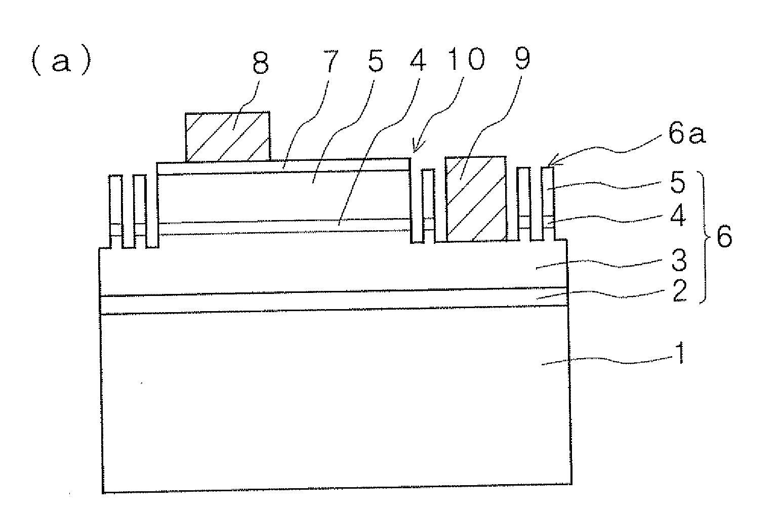
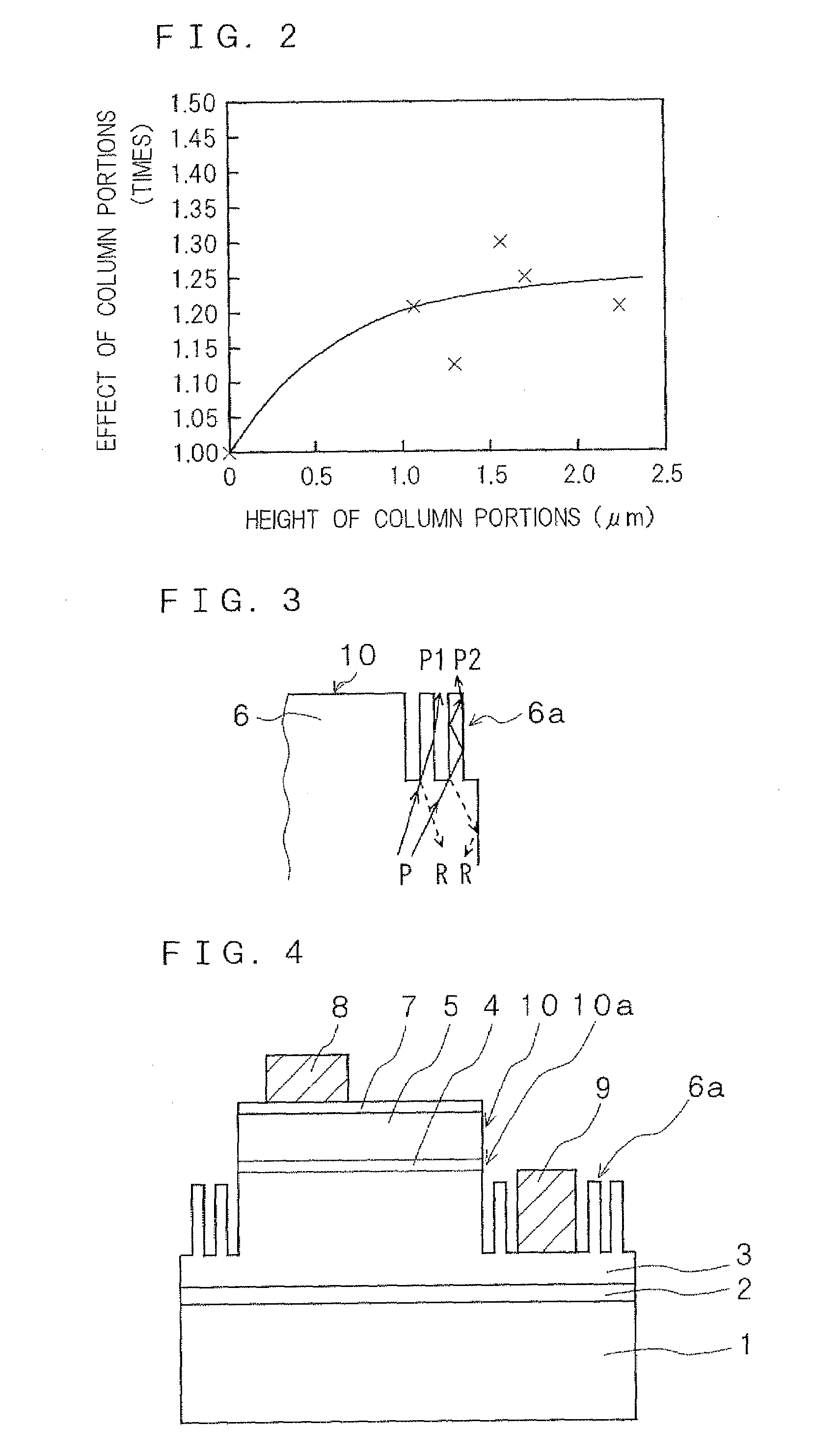
[0036]An explanation will be given below of a semiconductor light emitting device according to the present invention and a method for manufacturing the same in reference to the drawings. A cross-sectional view and a plan view explaining an embodiment of the semiconductor light emitting device according to the present invention in which nitride semiconductor layers suitable for emitting blue light are laminated on a sapphire substrate are shown in FIG. 1.

[0037]In the semiconductor light emitting device according to the present invention, as shown in FIG. 1, a semiconductor lamination portion 6 made of nitride semiconductor, including a first conductivity type layer and a second conductivity type layer, is laminated on a surface of a substrate 1 made of, for example, sapphire (single crystal of Al2O3) or the like. A first electrode (for example, p-side electrode 8) is provided so as to be electrically connected to the first conductivity type layer (for example, p-type layer 5) on a su...


PUM


Abstract

There are provided a nitride semiconductor light emitting device having a structure enabling enhanced external quantum efficiency by effectively taking out light which is apt to repeat total reflection within a semiconductor lamination portion and a substrate and attenuate, and a method for manufacturing the same. A semiconductor lamination portion (6) including a first conductivity type layer and a second conductivity type layer, made of nitride semiconductor, is provided on a surface of the substrate (1) made of, for example, sapphire or the like. A first electrode (for example, p-side electrode (8)) is provided electrically connected to the first conductivity type layer (for example, p-type layer (5)) on a surface side of the semiconductor lamination portion (6), and a second electrode (for example, n-side electrode (9)) is provided electrically connected to the second conductivity type layer (for example, n-type layer (3)). A part of the semiconductor lamination portion (6) is removed at a surrounding region of a chip of the semiconductor lamination portion (6) by etching so that column portions (6a) stand side by side by leaving the semiconductor lamination portion without etching, and the n-type layer (3) expose around the column portions (6a).

Description

FIELD OF THE INVENTION[0001]The present invention relates to a semiconductor light emitting device, in which nitride semiconductor layers are laminated on a substrate and emits blue type light (from ultraviolet rays to yellow light) and a method for manufacturing the same. More particularly, the present invention relates to a semiconductor light emitting device using nitride semiconductor and having a structure in which it is made easy to take out light reflected from a substrate side by forming unevenness on an exposed lower semiconductor layer, by leaving parts of a semiconductor lamination portion so as to stand side by side in a region, where a lower conductivity type layer of the semiconductor lamination portion is exposed by etching a part of the semiconductor lamination portion at least at a surrounding region of a chip, and relates to a method for manufacturing the same.BACKGROUND OF THE INVENTION[0002]As shown, for example, in FIG. 7, a semiconductor light emitting device e...

Claims


Application Information

Patent Timeline
Patent Type & Authority Applications(United States)
IPC IPC(8): H01L33/00H01L33/06H01L33/20H01L33/32
CPCH01L33/0079H01L33/60H01L33/20H01L33/0093
Inventor SAKAI, MITSUHIKOYAMAGUCHI, ATSUSHINAKAHARA, KENSONOBE, MASAYUKITSUTSUI, TSUYOSHI
Owner ROHM CO LTD
Why Eureka
Try Eureka