However, there are drawbacks to using MBC flash.
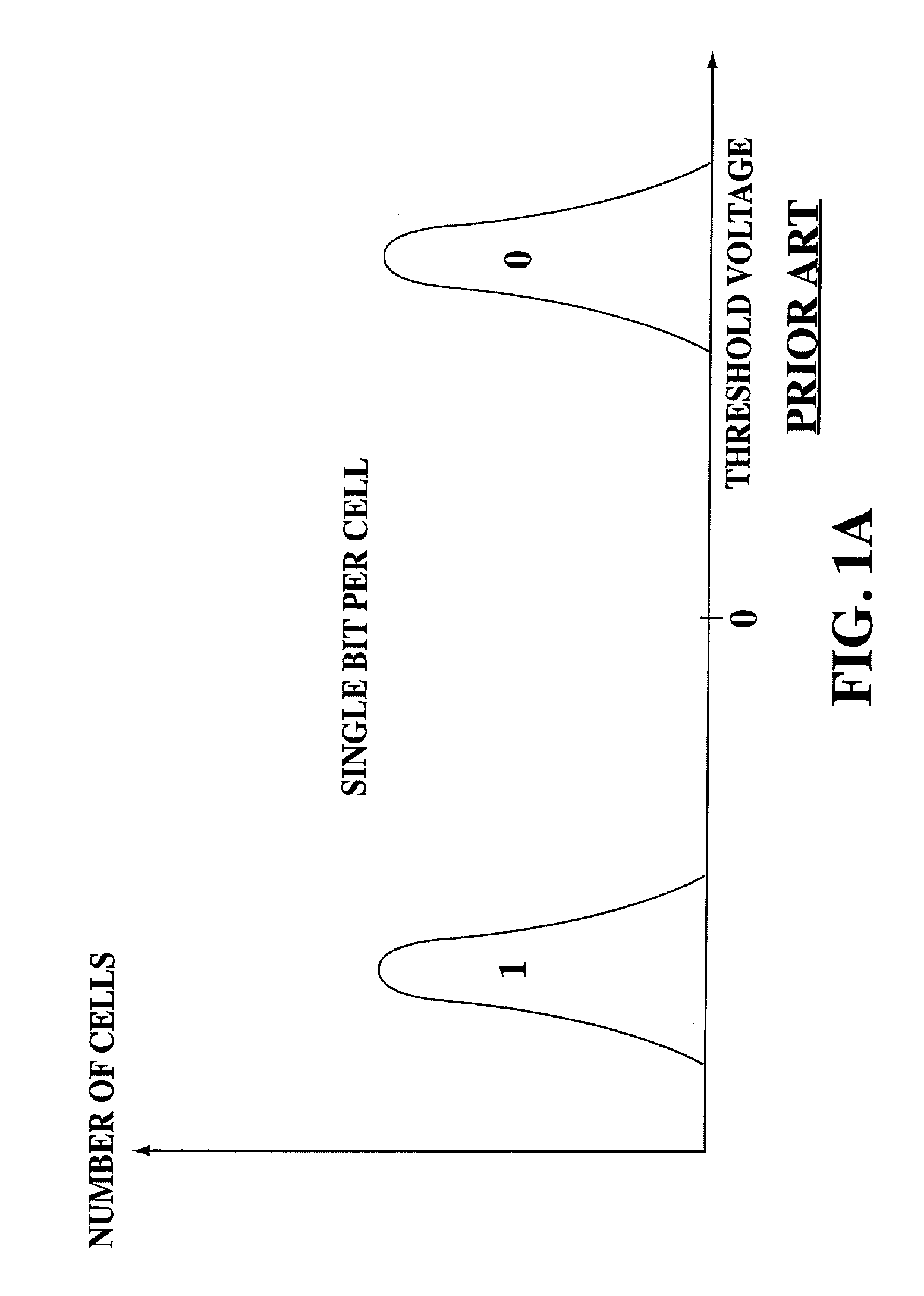
Average read and write times of MBC memories are longer than of SBC memories, resulting in worse performance.
Also, the reliability of MBC is lower than SBC.
Thus, a disturbance in the
threshold voltage (e.g leakage of stored charge causing a
threshold voltage drift or interference from operating neighboring cells) that are insignificant in SBC because of the large gap between the two states, may cause an MBC
cell to move from one state to another, resulting in an erroneous bit.
It is not possible to access any random address in the way described above for NOR—instead the host has to write into the device a sequence of bytes which identifies both the type of the requested command (e.g. read, write, erase, etc.) and the address to be used for that command.
Because of the non-
random access of NAND devices, they cannot be used for running code directly from the flash memory.
The SBC and MBC devices are not fully identical in their behavior—the time it takes to write an MBC page is much longer than time it takes to write an SBC page.
Typically, NAND devices are relatively difficult to interface and work with.
Another difficulty is the existence of errors in the data read from NAND devices, In contrast, NOR devices that can be assumed to always return correct data.
This inherent non-reliability of NAND devices requires the use of Error Detection Codes (EDC) and Error Correction Codes (ECC).
However, this architecture suffers from many disadvantages.
First, the host has to individually manipulate each one of the NAND device's control signals (e.g. CLE or ALE), which is cumbersome and time-consuming for the host.
Second, the support of EDC and ECC puts a severe burden on the host—parity bits have to be calculated for each page written, and error detection calculations (and sometimes also error correction calculations) must be performed by the host.
All this makes such “no controller” architecture relatively slow and inefficient.
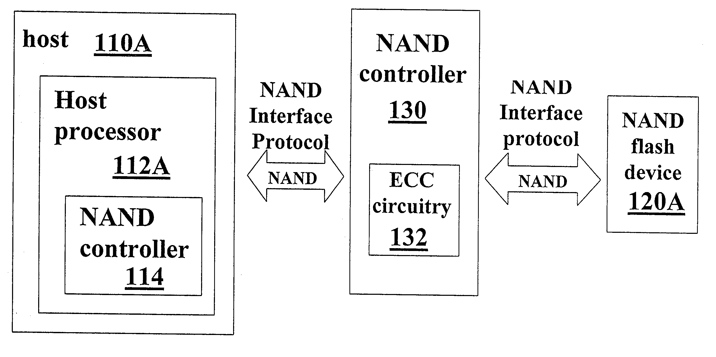
However, one cannot currently find a stand-alone NAND controller that exports NAND interface to the host.
The prior art described above leaves one problem unsolved.
This is so because a NAND controller provides a certain level of
error detection and correction, and therefore cannot support NAND devices with lower reliability.
Such controller cannot work with two-bit-per-
cell MBC NAND devices because they require 4-bit ECC, and therefore some data might not be read correctly into the processor.
Similarly, a NAND controller providing 4-bit ECC can work with current two-bit-per-cell MBC NAND, but will not work with next generation MBC NAND devices that will most probably require a higher level of ECC capability.
This is so because future MBC NAND devices are expected to be less reliable than current MBC devices and to require a much stronger ECC capability.
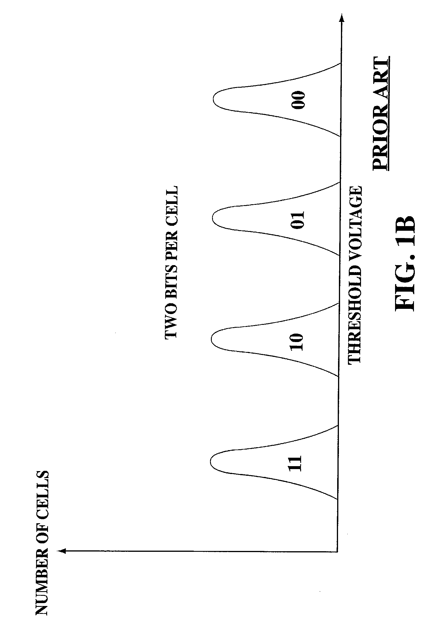
a. The process used for manufacturing NAND devices is continuously being improved to yield smaller memory cells. While a few years ago NAND devices used 0.4 micron process, currently they use 90 nm and 70 nm technology, and this shrinking trend is expected to continue. With shrinking dimensions of the memory cells comes lower reliability, as the small dimensions make the cells more sensitive to physical effects and phenomena that previously were not important.
b. When MBC cells with more than two bits per cell will become commercially available, they will necessarily be much less reliable than SBC cells and two-bit-per-cell MBC cells. The larger number of states that have to be represented by the cell's
threshold voltage imply that the margins between states are smaller and even smaller disturbances and drifts result in incorrect reading of data. This effect could already be witnessed in the comparison between SLC and two-bit-per-cell MBC, where the ECC requirements increased from 1-bit ECC to 4-bit ECC.
If the MBC NAND is connected to the NAND interface of the built-in controller of the processor, which might be the only way to connect it to the processor, then the MBC NAND generates too many errors for the limited-capability ECC of the built-in controller to correct.
But when NAND devices with lower reliability appear in the market, the processor is not able to benefit from their lower price because its built-in controller is not able to provide the required level of error correction.
Therefore we see that the state of the prior art does not provide a good solution to the problem of benefiting from the cost
advantage of a new NAND device, while using a
host processor incorporating a built-in NAND controller designed to support a
previous generation of NAND devices.

