Light-emitting device containing a composite electroplated substrate

Inactive Publication Date: 2010-02-04
EPISTAR CORP
View PDF5 Cites 11 Cited by
  • Summary
  • Abstract
  • Description
  • Claims
  • Application Information

AI Technical Summary

Benefits of technology

[0015]In one embodiment of the present application, a light-emitting diode comprises a multiple-film layer stacked alternately by multiple high strength films and multiple

Problems solved by technology

However, due to the difference of the thermal expansion coefficients of materials, the light-emitting diode wafer often cracks during the manufactur

Method used


Image

  • Light-emitting device containing a composite electroplated substrate
  • Light-emitting device containing a composite electroplated substrate
  • Light-emitting device containing a composite electroplated substrate

Examples


Example

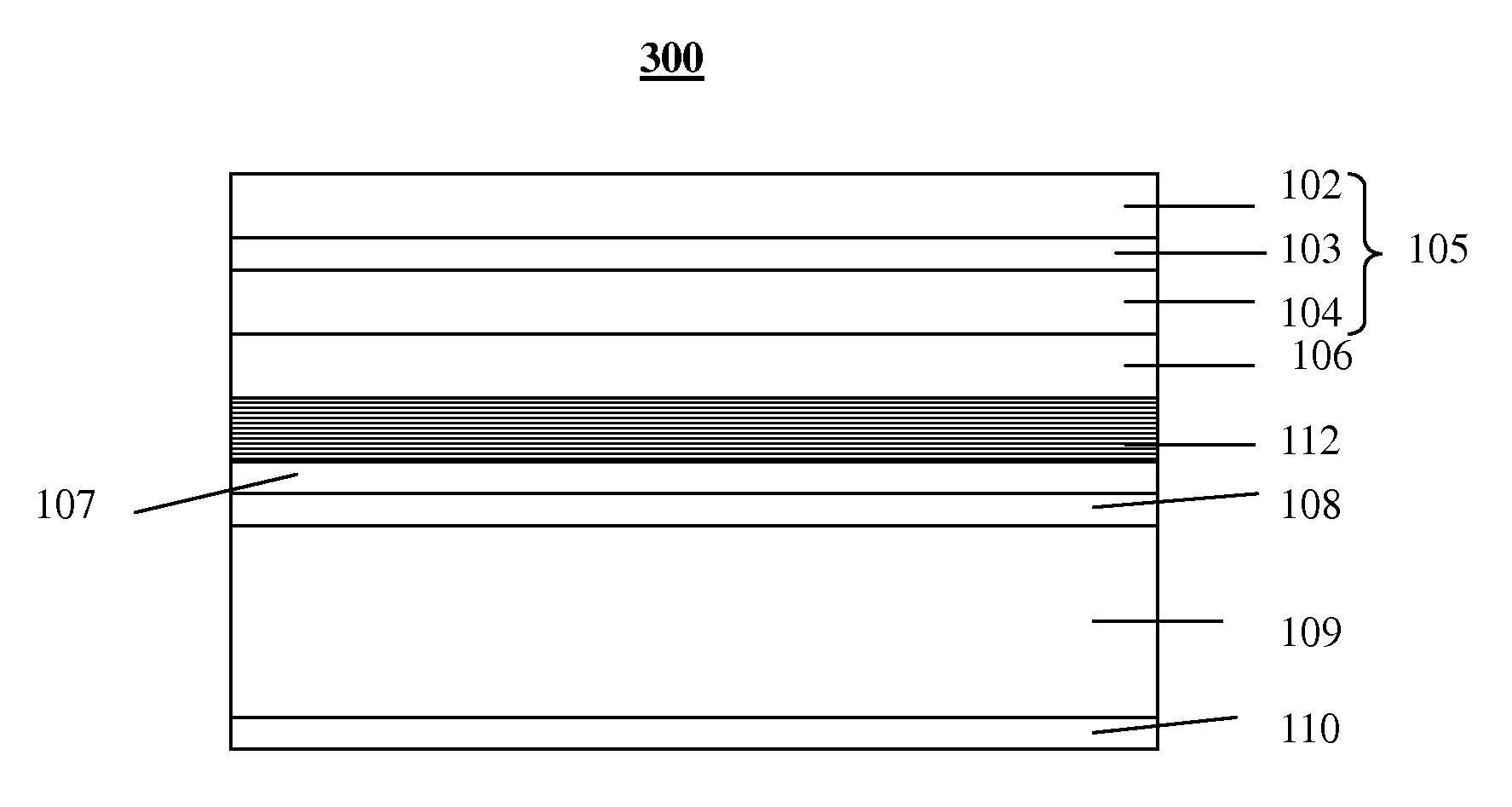
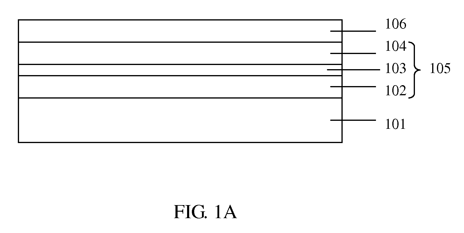
[0020]The first embodiment of the present application is illustrated in FIG. 1A to FIG. 1F. Referring to FIG. 1A, a growth substrate 101 is provided. A semiconductor epitaxy structure 105 is formed on the growth substrate, included at least a first conductivity type semiconductor layer 102, an active layer 103, and a second conductivity type semiconductor layer 104. In this embodiment, the first conductivity type semiconductor layer 102 is an n-GaN layer, the active layer 103 is an InGaN / GaN multiple quantum wells structure, and the second conductivity type semiconductor layer 104 is a p-GaN layer. The semiconductor epitaxy structure 105 is formed on sapphire by the epitaxy technology. The reflective layer 106 is formed on the semiconductor epitaxy structure 105 as a stack of titanium (thickness is 30 nm) / aluminum (thickness is 200 nm). It can also be as a stack of titanium / gold or titanium / silver.

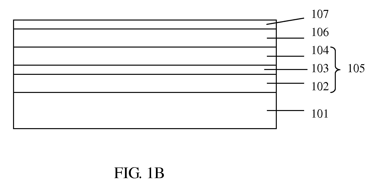
[0021]Referring to FIG. 1B, a seed layer 107 is formed on the reflective layer 106 to ...


PUM


Abstract

The application is related to a method of forming a substrate of a light-emitting diode by composite electroplating. The application illustrates a light-emitting diode comprising the following elements: a light-emitting epitaxy structure, a reflective layer disposed on the light-emitting epitaxy structure, a seed layer disposed on the reflective layer, a composite electroplating substrate disposed on the seed layer by composite electroplating, and a protection layer disposed on the composite electroplating substrate.

Description

CROSS REFERENCE TO RELATED APPLICATIONS[0001]This application claims the right of priority based on Taiwan Patent Application No. 097129481 entitled “A Light-Emitting Device Containing a Composite Electroplated Substrate”, filed on Aug. 1, 2008, which is incorporated herein by reference and assigned to the assignee herein.TECHNICAL FIELD[0002]The present application generally relates to a light-emitting device, and more particularly to a light-emitting diode comprising a composite electroplated substrate.BACKGROUND[0003]The vertical type light-emitting diodes (LEDs) become a popular choice to light-emitting diodes package for its simple design, high power, high efficiency, and long life-time. To optimize the heat dispersion, the light-emitting diodes are usually attached to the metal substrate by bonding technology, or by electroplating technology to evaporate metal film on the epitaxy layers. However, due to the difference of the thermal expansion coefficients of materials, the lig...

Claims


Application Information

Patent Timeline
IPC IPC(8): H01L33/00
CPCH01L33/0079H01L33/46H01L33/405H01L33/0093
Inventor HSU, CHIA-LIANGHSIEH, MIN-HSUNLU, CHIH-CHIANGHUANG, CHIEN-FU
Owner EPISTAR CORP
Why Eureka
Try Eureka