Check patentability & draft patents in minutes with Patsnap Eureka AI!

Fluorescence detection system and method

Inactive Publication Date: 2010-02-11
GENERAL ELECTRIC CO
View PDF19 Cites 27 Cited by
  • Summary
  • Abstract
  • Description
  • Claims
  • Application Information

AI Technical Summary

Problems solved by technology

However, such a small-scale analysis causes very high requirements on its detection system in terms of sensitivity and selectivity etc.
However, it is time-consuming and cost-ineffective to embed the waveguides and the optics devices in a very small microfluidic chip.
Moreover, it is very difficult to replace any parts of the detection system without a complicated alignment and calibration.
In addition, the LIF detection system has fibers to couple with and to deliver the excitation light into the respective waveguides, it further adds more complexity to the microfluidic chip fabrication due to the matching requirement of the fibers coupling with the respective waveguides in numerical aperture and in fiber core and waveguide size.

Method used


Image

  • Fluorescence detection system and method
  • Fluorescence detection system and method
  • Fluorescence detection system and method

Examples


Embodiment Construction

[0020]Preferred embodiments of the present disclosure will be described hereinbelow with reference to the accompanying drawings. In the following description, well-known functions or constructions are not described in detail to avoid obscuring the disclosure in unnecessary detail.

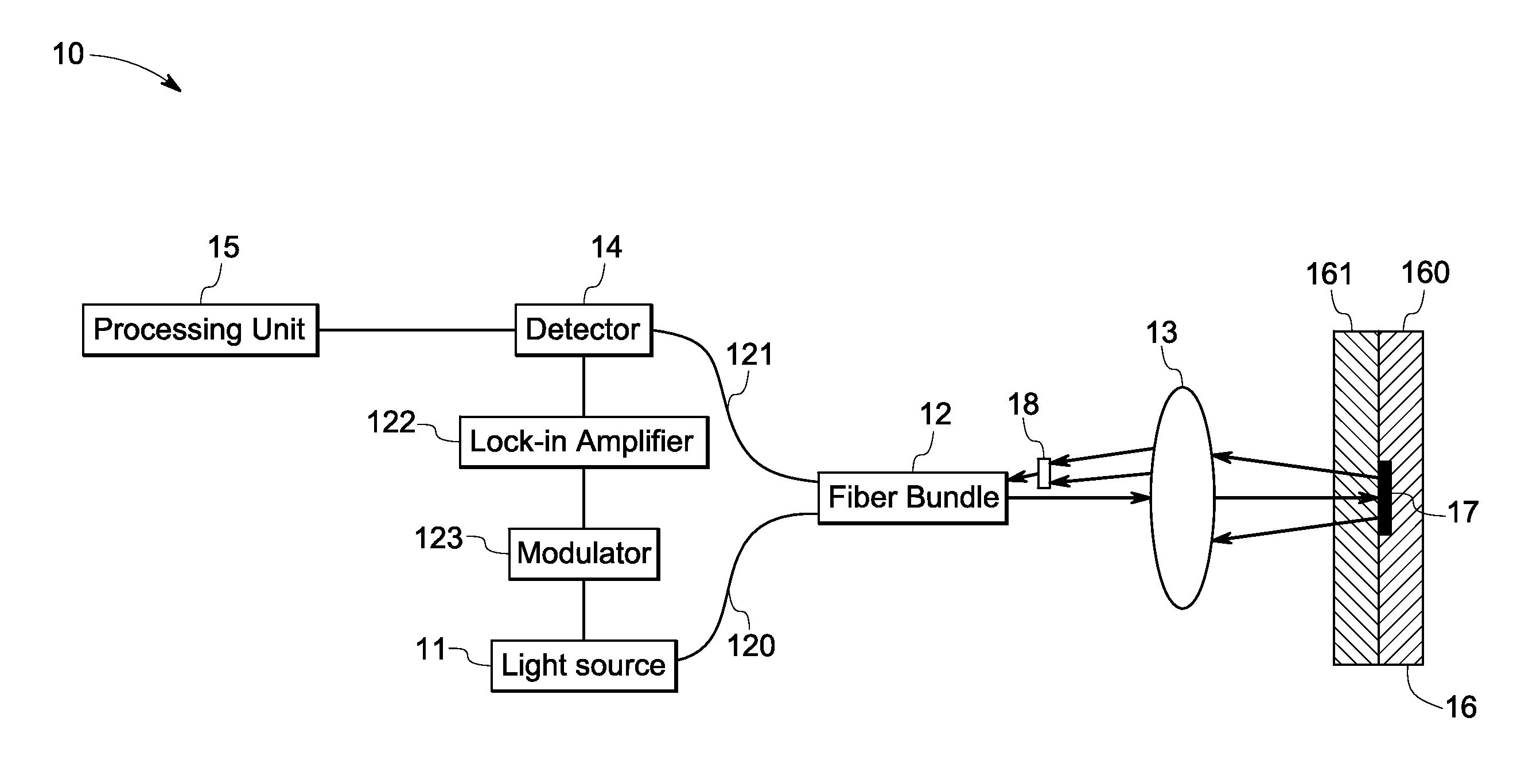
[0021]FIG. 1 illustrated a schematic diagram of a fluorescence detection system 10 in accordance with one embodiment of the invention. The fluorescence detection system 10 comprises a light source 11, a fiber bundle probe 12, an optical lens 13, a detector 14 and a processing unit 15. In embodiments of the invention, the light source 11 comprises a frequency modulated laser source or a light emitting diode (LED) source with a laser light fiber. The fiber bundle probe 12 comprises a transmitting fiber 120 and at least one receiving fiber 121. The optical lens 13 comprises a microscope objective or an aspheric lens. The detector 14 comprises a silicon-based photo detector or an avalanche photodiode detector, ...


PUM


Abstract

A fluorescence detection system comprises a light source configured to produce an excitation light, an optical lens and a fiber bundle. The optical lens is configured to focus the excitation light to a sample to emit fluorescence and to collect the fluorescence. The fiber bundle probe comprises a transmitting fiber configured to transmit the excitation light to the optical lens, and a first receiving fiber configured to deliver the collected fluorescence. The fluorescence detection system further comprises a first detector configured to detect the fluorescence delivered by the receiving fiber to generate a response signal, and a processing unit configured to determine information about the samples by analyzing the response signal. Additionally, a fluorescence detection method is also presented.

Description

BACKGROUND[0001]This invention relates generally to a fluorescence detection system and a method for detecting fluorescence. More particularly, this invention relates to a fluorescence detection system for a lab-on-a-chip and a method for detecting fluorescence from the lab-on-a-chip.[0002]A lab-on-a-chip, also named a microfluidic chip or a microchip, is a miniaturized device for manipulating and analyzing chemical / biological samples in micrometer-sized channels thereof. The lab-on-a-chip can be fabricated by a micro-machining techniques, such as photolithography, wet etching, or laser ablation, and is referred to as a chemical / biological microprocessor including a variety of processes (such as sample pretreatment, injection, reaction, separation and detection) integrated in a glass, silicon, or plastic substrate of an area of several square centimeters. It offers faster analysis while using much smaller amount of samples and reagents, usually on a micro-liter scale. This microflui...

Claims


Application Information

Patent Timeline
IPC IPC(8): G01N21/64
CPCB01L3/5027G01J3/02G01J3/0208G01J3/0218G01J3/08G01N2201/0833G01N21/6408G01N21/645G01N2021/6419G01N2021/6484G01N2201/0826G01J3/4406
Inventor XIA, HUAZHU, LIBARASH, EUGENEFINEHOUT, ERIN JEANPIETRZYKOWSKI, MATTHEW DAMIAN
Owner GENERAL ELECTRIC CO
Features
  • R&D
  • Intellectual Property
  • Life Sciences
  • Materials
  • Tech Scout
  • Unparalleled Data Quality
  • Higher Quality Content
  • 60% Fewer Hallucinations
Learn More