Techniques for Mounting a Millimeter Wave Antenna and a Radio Frequency Integrated Circuit Onto a PCB

a technology millimeter wave antenna, which is applied in the field of radio frequency integrated circuit, can solve the problems of inability to use dipole antennas on chips, inability to provide 360-degree spectrum coverage of antennas, and loss of energy, and achieve the effect of shortening the length of traces

Inactive Publication Date: 2010-02-11
QUALCOMM INC
View PDF12 Cites 20 Cited by
  • Summary
  • Abstract
  • Description
  • Claims
  • Application Information

AI Technical Summary

Benefits of technology

[0017]Certain embodiments of the invention include a printed circuit board (PCB) assembled to include at least one millimeter wave antenna and a radio frequency integrated circuit (RF IC). The PCB comprises a square-shaped cavity in the PCB, wherein one of the edges of the cavity is substantially parallel to connecting pins of the at least one millimeter wave antenna; a RF IC placed in the cavity, wherein one side of the RF IC including RF pads is substantially at the edge of the cavity that is substantially parallel to the connecting pins; and traces connecting the RF pads and the connecting pins, wherein the connection between the at least one millimeter wave antenna and the RF IC shortens the length of the traces.

Problems solved by technology

Most of the energy is lost due to the connection between an antenna and an integrated circuit (IC), or chip, processing the RF signals to be transmitted or received.
In addition, the antenna 100 does not provide spectrum coverage of 360 degrees.
The on-chip dipole antenna 100 is not feasible for commercial uses due to its inefficiency.
This is due to the substrate and connection losses.
However, the LTCC process is very costly, and therefore is not feasible for commercial uses.

Method used


Image

  • Techniques for Mounting a Millimeter Wave Antenna and a Radio Frequency Integrated Circuit Onto a PCB
  • Techniques for Mounting a Millimeter Wave Antenna and a Radio Frequency Integrated Circuit Onto a PCB
  • Techniques for Mounting a Millimeter Wave Antenna and a Radio Frequency Integrated Circuit Onto a PCB

Examples


Embodiment Construction

[0020]The subject matter that is regarded as the invention is particularly pointed out and distinctly claimed in the claims at the conclusion of the specification. The foregoing and other objects, features and advantages of the invention will be apparent from the following detailed description taken in conjunction with the accompanying drawings.

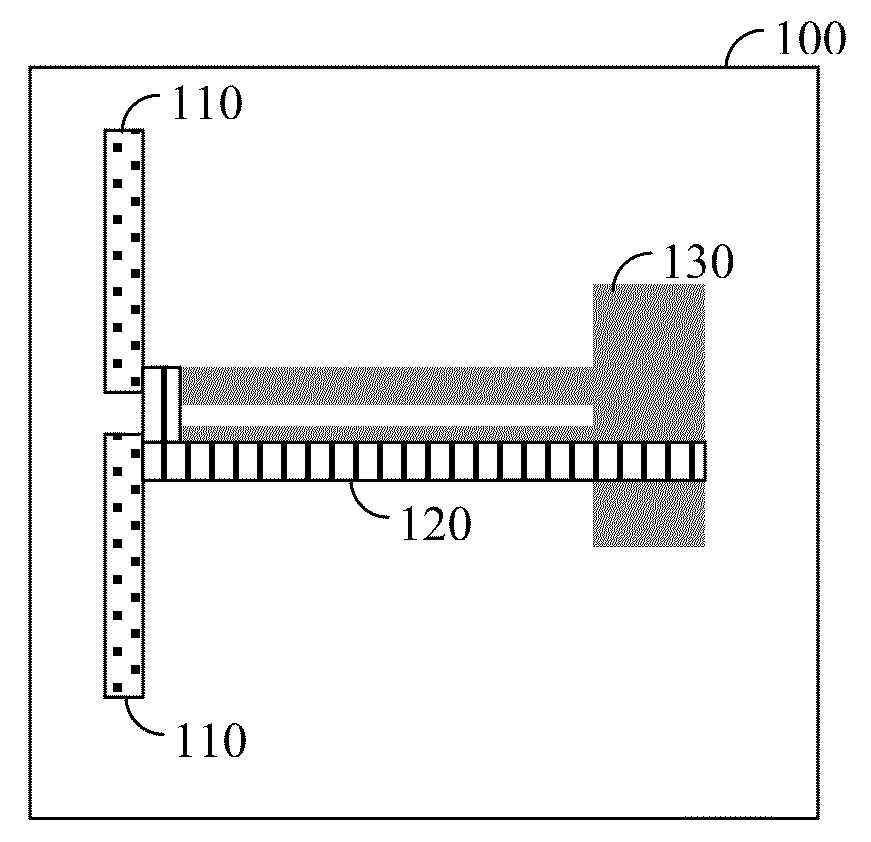
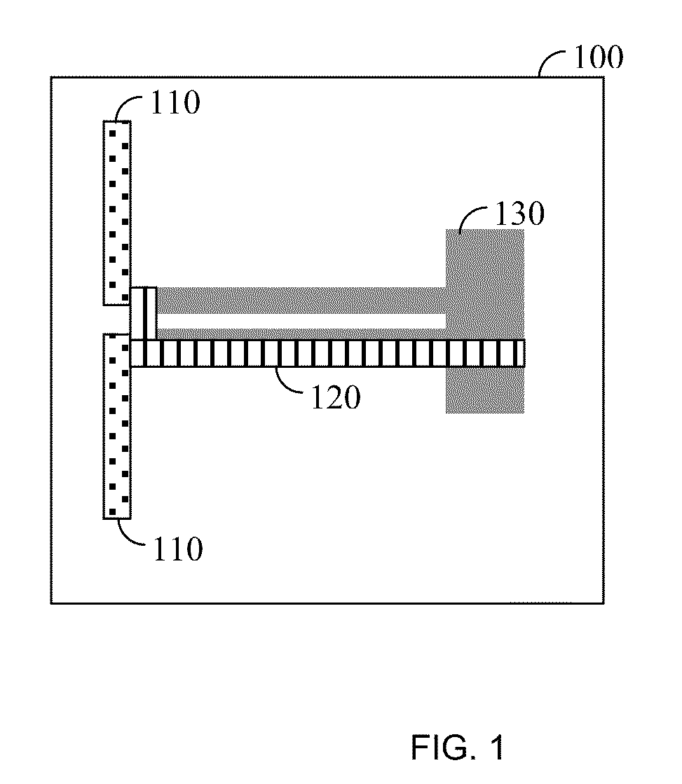
[0021]Certain embodiments of the invention include a method for mounting a millimeter wave antenna and a RF IC onto a PCB. Certain embodiments of the method reduce the energy lost on the connection between these two circuits. Other embodiments of the invention include a quasi-omnidirectional (omni) millimeter wave antenna, and a method of manufacture. Certain embodiments of the invention enable a mass production of low-cost and high performance RF devices that can be utilized in millimeter wave bands including, but not limited to, 60 GHz and 77 GHz.

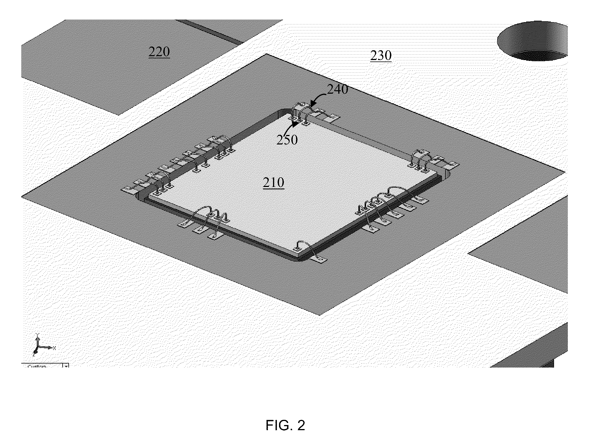
[0022]FIG. 2 shows a three-dimensional diagram illustrating the assembly of a RF IC 210 and a m...


PUM

PropertyMeasurementUnit
lengthaaaaaaaaaa
frequencyaaaaaaaaaa
heightaaaaaaaaaa

Abstract

A printed circuit board (PCB) assembled to include at least one millimeter wave antenna and a radio frequency integrated circuit (RF IC). The PCB comprises a square-shaped cavity in the PCB, wherein one of the edges of the cavity is substantially parallel to connecting pins of the at least one millimeter wave antenna; a RF IC placed in the cavity, wherein one side of the RF IC including RF pads is substantially at the edge of the cavity that is substantially parallel to the connecting pins; and traces connecting the RF pads and the connecting pins, wherein the connection between the at least one millimeter wave antenna and the RF IC shortens the length of the traces.

Description

CROSS-REFERENCE TO RELATED APPLICATION[0001]This application claims the benefit of U.S. provisional application No. 61 / 086,924 filed on Aug. 7, 2008, the contents of which are herein incorporated by reference.TECHNICAL FIELD[0002]The present invention relates generally to radio frequency integrated circuits, and particularly to connecting radio frequency integrated circuits to millimeter wave antennas.BACKGROUND OF THE INVENTION[0003]The 60 Giga Hertz (GHz) band is an unlicensed band which features a large amount of bandwidth allowing a very high volume of information to be transmitted wirelessly. As a result, multiple applications, that require transmission of a large amount of data, can be developed to allow wireless communication around the 60 GHz band. Examples for such applications include, but are not limited to, a wireless high definition TV (HDTV), a wireless docking station, a wireless Gigabit Ethernet, and many others.[0004]In order to facilitate such applications there is...

Claims


Application Information

Patent Timeline
Patent Type & Authority Applications(United States)
IPC IPC(8): H01Q1/00H01Q9/16
CPCH01Q1/22H01Q3/24Y10T29/49826H04B7/26H01Q9/285
Inventor MYSZNE, JORGESHEMESH, YAIR
Owner QUALCOMM INC
Why Eureka
Try Eureka