Light emitting and lasing semiconductor devices and methods

a technology of semiconductor devices and semiconductor lasers, applied in semiconductor lasers, semiconductor devices, laser details, etc., can solve the problems of resonance peak and speed limitation, avoid injection and transport, sluggish, and high mass

Active Publication Date: 2010-02-11
THE BOARD OF TRUSTEES OF THE UNIV OF ILLINOIS
View PDF7 Cites 47 Cited by
  • Summary
  • Abstract
  • Description
  • Claims
  • Application Information

AI Technical Summary

Benefits of technology

[0009]An advantage of the invented device structure and method, is that the EM field confinement on the collector side (bottom side of the base) can be shifted down into the “collector” body and thus allow “tuning” of the EM field to maximize the stimulated recombination (emission) at the position of the base QW(s). The appropriate high doping of the p-type “base” region is not necessarily limiting. This is known from the extremely high acceptor doping of the original diffused junction diode lasers (GaAs and GaAsP), and from the subsequent tunnel-contact edge emitting and vertical cavity lasers, and more recently, transistor lasers. Thus, it is possible to dope-in holes in high performance lasers, and avoid the injection and transport of holes, which are high in mass, sluggish, and poorly conducting. This is a part of the structure and technique of a form of the invention. The two terminal device hereof is simpler in some respects than a three terminal transistor, with its need for a lateral base contact. The two terminal device can be made relatively smaller and faster.

Problems solved by technology

Inevitably, at high enough speed, the charge-photon interaction leads to a resonance peak and speed limitation.

Method used


Image

  • Light emitting and lasing semiconductor devices and methods
  • Light emitting and lasing semiconductor devices and methods
  • Light emitting and lasing semiconductor devices and methods

Examples


Embodiment Construction

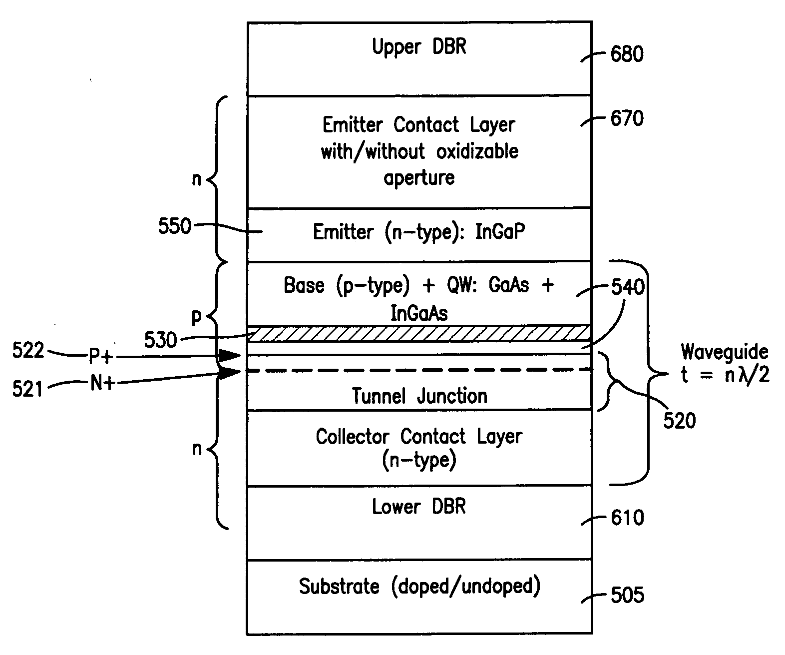
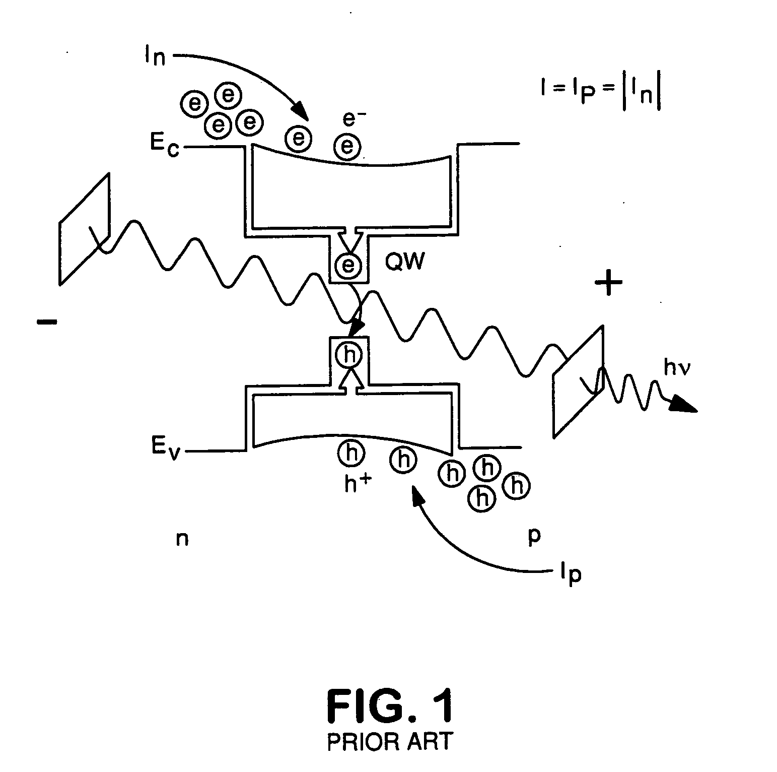
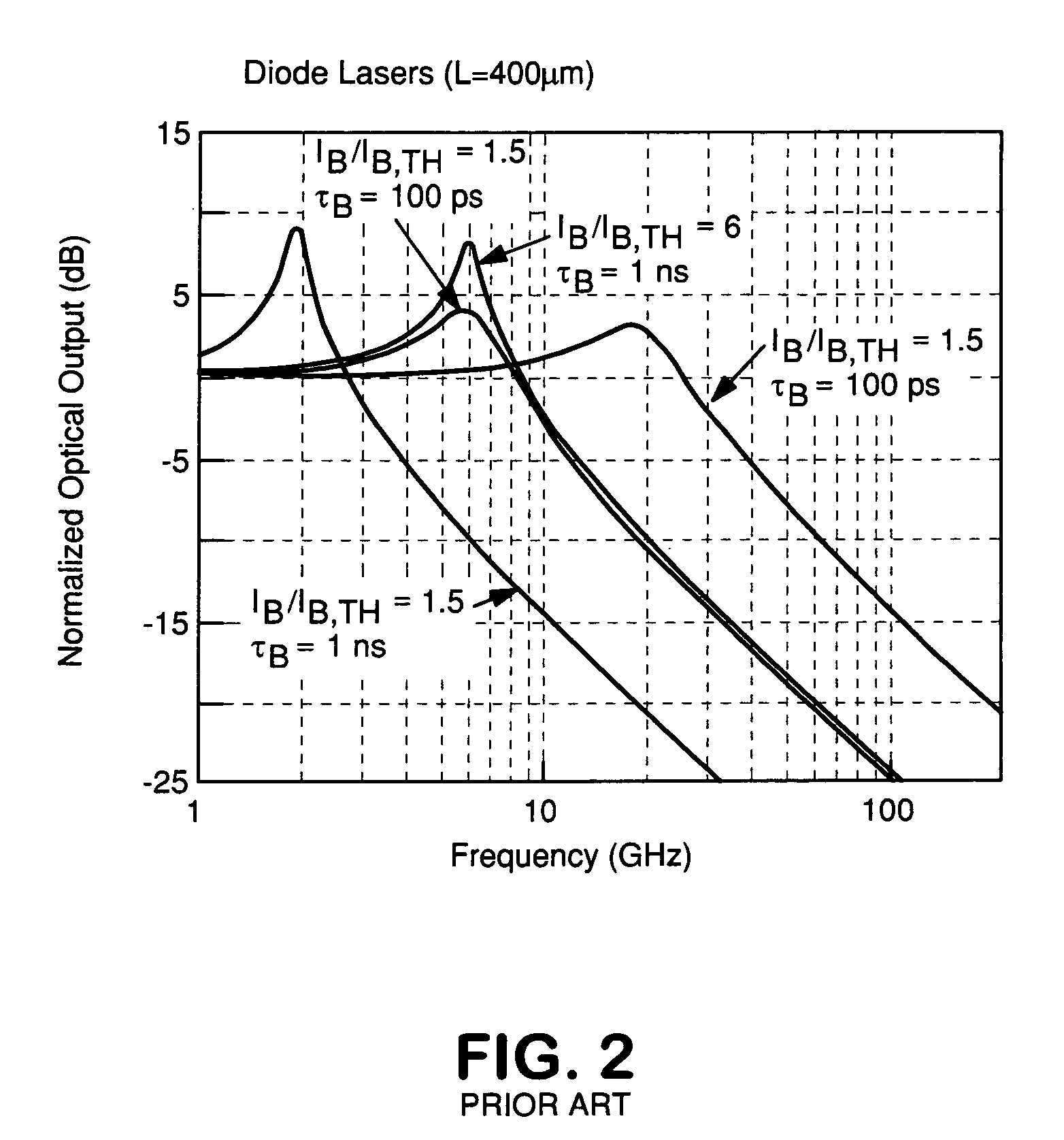
[0028]In approaching the problem of improving the operating speed of existing HBT laser diodes, we start by further analyzing operation of our transistor laser, which is first mentioned in the Background section hereof. A form of the transistor laser is an n-p-n heterojunction bipolar transistor, an n-p-n HBT, with electrons injected at the emitter and transporting efficiently (easily, low mass, high mobility) by diffusion to the collector. The injected electrons are essentially tilted, by diffusion, into a triangular distribution pinned at zero concentration at the base-collector junction. Holes in III-V crystals are high mass and sluggish, and are built-in (acceptor doping), at high concentration, in the p+ base. For a transistor to be a transistor some electrons recombine with holes in the base (IB≠0 and IE=IB+IC, giving gain β=IC / IB), the lost positive charge being resupplied by dielectric relaxation (not injection) by the base contact. It is emphasized that the holes are not in...


PUM


Abstract

A two terminal semiconductor device for producing light emission in response to electrical signals, includes: a terminal-less semiconductor base region disposed between a semiconductor emitter region and a semiconductor collector region having a tunnel junction adjacent the base region; the base region having a region therein exhibiting quantum size effects; an emitter terminal and a collector terminal respectively coupled with the emitter region and the collector region; whereby application of the electrical signals with respect to the emitter and collector terminals, causes light emission from the base region. Application of the electrical signals is operative to reverse bias the tunnel junction. Holes generated at the tunnel junction recombine in the base region with electrons flowing into the base region, resulting in the light emission. The region exhibiting quantum size effects is operative to aid recombination.

Description

PRIORITY CLAIM[0001]Priority is claimed from U.S. Provisional Patent Application No. 60 / 998,645, filed Oct. 12, 2007, and said U.S. Provisional Patent Application is incorporated herein by reference.GOVERNMENT SUPPORT[0002]This invention was made with government support under DARPA Contract Number HR0011-04-1-0034, and the government has certain rights in the invention.FIELD OF THE INVENTION[0003]This invention relates to two terminal semiconductor devices for producing light emission and laser emission in response to electrical signals. The invention also relates to methods for producing light emission and laser emission from semiconductor devices, including such emission that can be controlled with very fast response time.BACKGROUND OF THE INVENTION[0004]A part of the background hereof lies in the development of light emitters based on direct bandgap semiconductors such as III-V semiconductors. Such devices, including light emitting diodes and laser diodes, are in widespread comme...

Claims


Application Information

Patent Timeline
Patent Type & Authority Applications(United States)
IPC IPC(8): H01S5/00H01L33/00
CPCH01S5/3095H01S5/06203
Inventor HOLONYAK, JR., NICKFENG, MILTONWALTER, GABRIELJAMES, ADAM
Owner THE BOARD OF TRUSTEES OF THE UNIV OF ILLINOIS
Why Eureka
Try Eureka