Crystalline silicon substrates with improved minority carrier lifetime

Inactive Publication Date: 2010-02-11
GLOBALFOUNDRIES INC
View PDF9 Cites 3 Cited by
  • Summary
  • Abstract
  • Description
  • Claims
  • Application Information

AI Technical Summary

Benefits of technology

[0004]In accordance with the present invention, a method for improving the minority carrier lifetime of a silicon containing substrate or semiconductor wafer having metallic contaminants therein comprises annealing the wafer at a temperature in the range from about 1200° C. to about 1375° C. in a gaseous ambient of oxygen, an inert gas and a chlorine containing gas such as HCl for a time period in the range from about 1 minute to about 50 hours whereby the metallic contaminants form volatile metal chlorides and evaporate from the wafer. Concurrently, an oxide layer may be formed on the surface of the silicon containing substrate or semiconductor wafer.
[0005]The invention further provides annealing as described above at a temperature at or above 1200° C. to improve lifetime which may be the result of dissolved SiOx precipitates, metal and other contaminant gettering, and other crystallographic or point defect migration related phenomena.
[0007]The invention therefore provides a process to improve the minority carrier lifetime in scrapped silicon containing substrates or semiconductor wafers up to a level comparable to that of solar grade material. The treated scrapped wafers can then be used for fabricating solar cells with efficiencies similar to those of solar grade silicon.

Problems solved by technology

A major drawback that prevents the large spread use of solar cells is the cost of photovoltaic material, which is presently about 40% to 50% of the final product.
If the starting material comprises scrapped silicon wafers from an MOS FET production line, the wafers have a cost which is just of a few percent of the cost of solar grade Si wafers.
Because of the low minority carrier lifetime (<few microseconds) of scrapped silicon wafers, the solar efficiency for photovoltaic conversion of a cell made with this silicon material is less than 14% efficient.

Method used


Image

  • Crystalline silicon substrates with improved minority carrier lifetime
  • Crystalline silicon substrates with improved minority carrier lifetime
  • Crystalline silicon substrates with improved minority carrier lifetime

Examples


Embodiment Construction

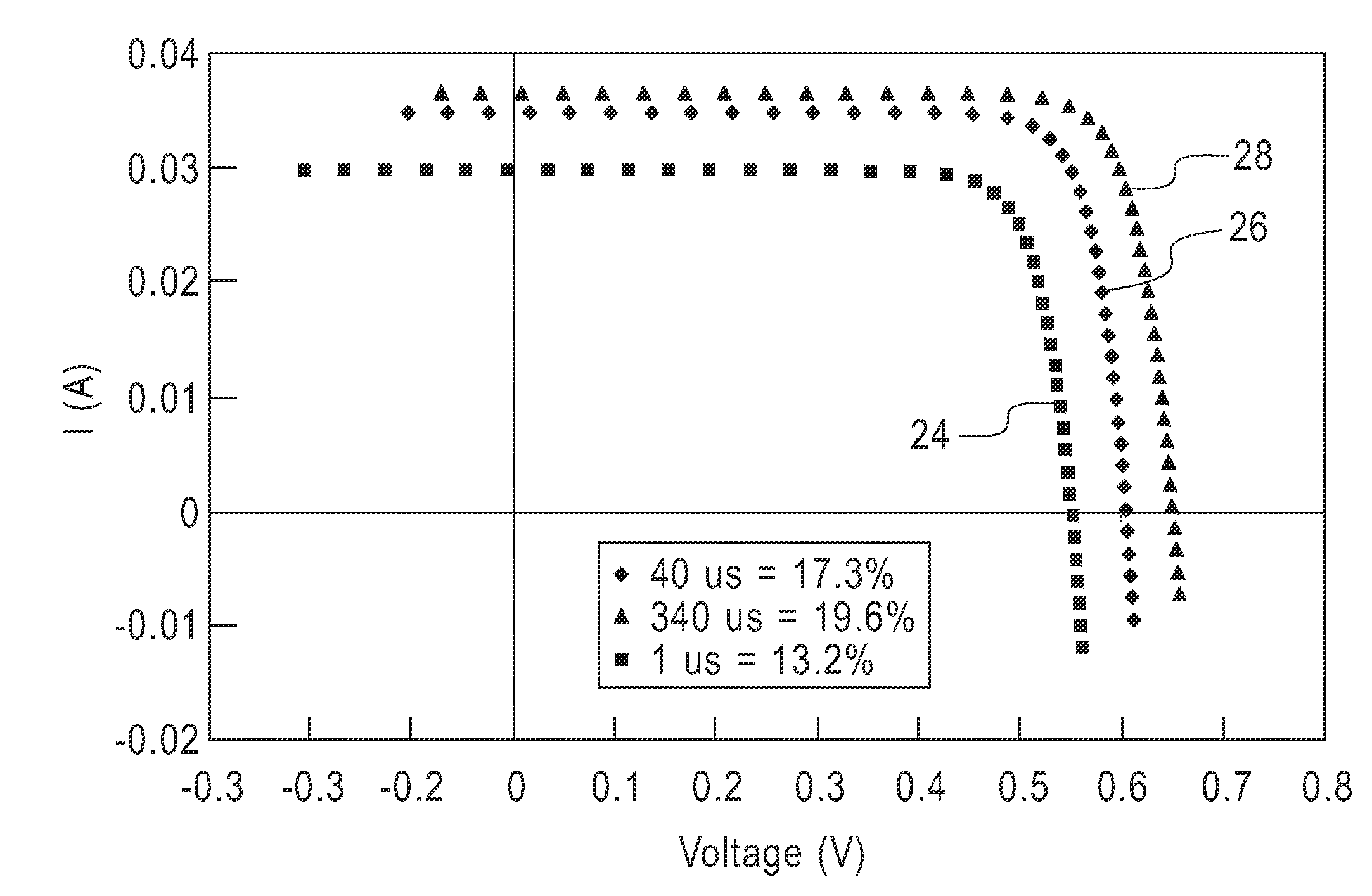
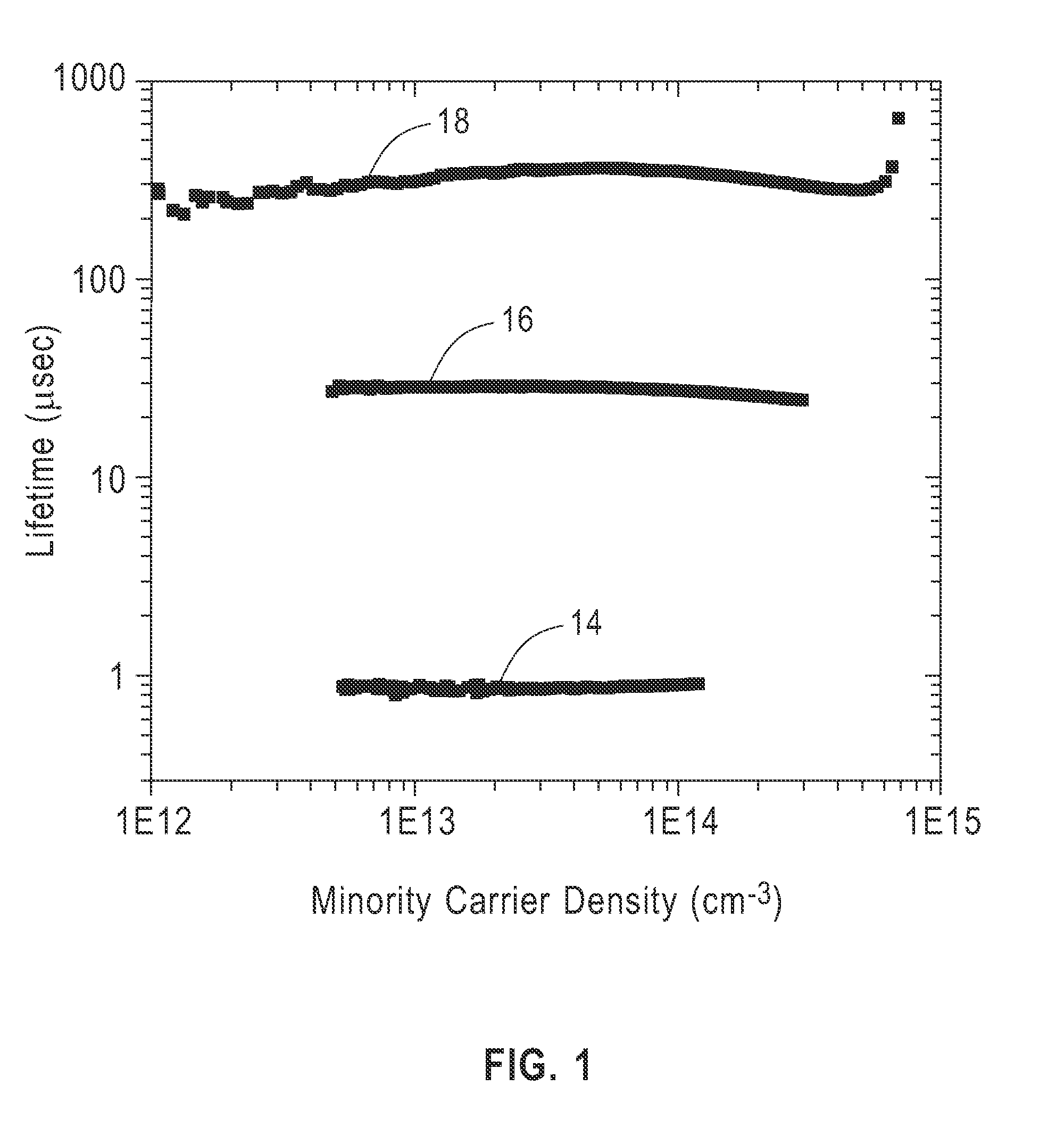
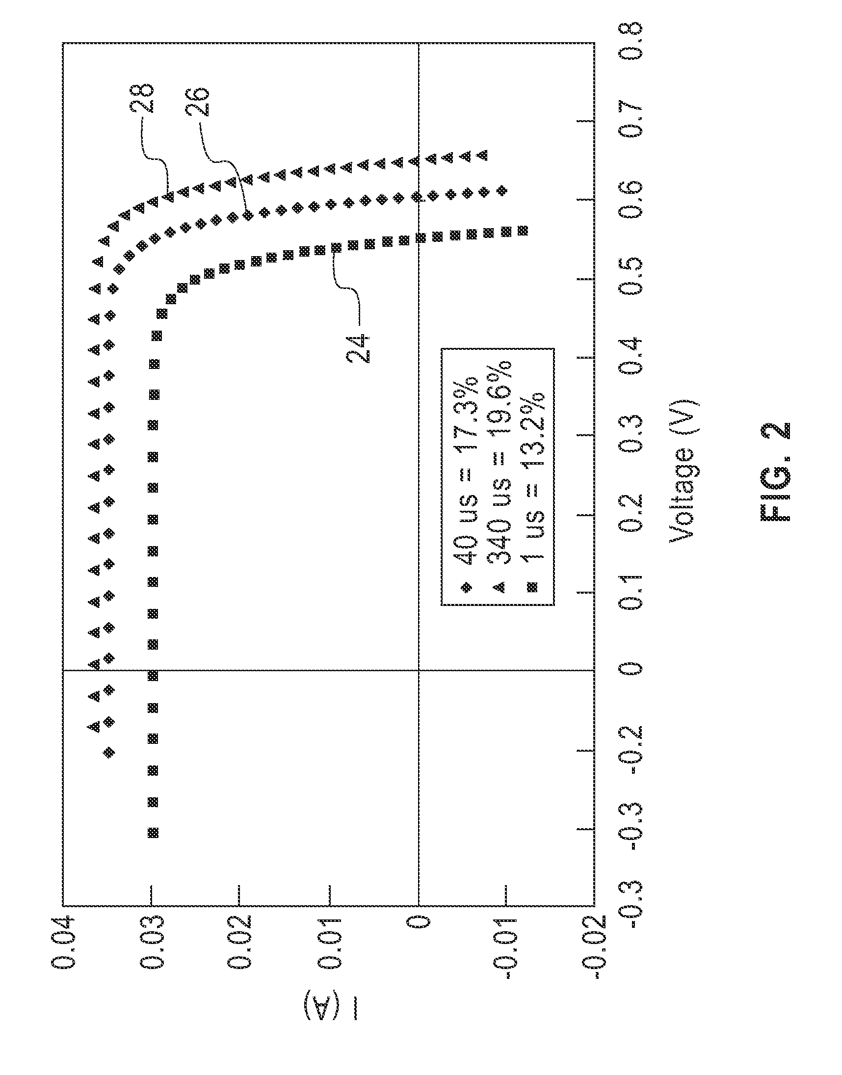
[0011]In order to increase the lifetime in scrapped Si containing wafers, the upper portion of the wafer is removed which may contain doped regions, MOS FETs and / or bipolar transistors and interconnection wiring. The scrapped wafers may be single crystalline, poly crystalline or Silicon-on-Insulator (SOI) and have a minority carrier lifetime less than 10 microseconds. The scrapped wafers may be semiconductor wafers selected from the group consisting of CMOS grade Si wafers, Si scrapped wafers from CMOS processing, solar grade single crystal Si wafers, solar grade multi-crystalline Si wafers and other types of defective Si wafers having crystallographic defects comprising one or more of twins, stacking faults, point defects, dislocations, precipitates and oxygen interstitial defects. A chemical etch may be performed on the upper surface of the Si containing wafer to remove several micrometers such as 0.01 micrometers to 30 micrometers and preferably about 20 micrometers which may con...


PUM


Abstract

A method for improving the minority lifetime of silicon containing wafer having metallic contaminants therein is described incorporating annealing at 1200° C. or greater and providing a gaseous ambient of oxygen, an inert gas and a chlorine containing gas such as HCl.

Description

FIELD OF THE INVENTION[0001]The present invention relates to improving the minority carrier lifetime of silicon containing substrates or wafers and more particularly to removing metal impurities and SiOx precipitates from scrapped substrates that may have contained MOS FETs for reuse, for example, for fabricating solar cells.BACKGROUND OF THE INVENTION[0002]A major drawback that prevents the large spread use of solar cells is the cost of photovoltaic material, which is presently about 40% to 50% of the final product. There are several approaches that have been tried to minimize the cost of photovoltaic material. The large majority of these approaches are directed to reducing the price of the material by reducing the amount of material used in the solar cell. In other words, fabricate a solar cell on a thin silicon film. The thin silicon films are deposited on top of glasses or on other low cost material, which limit the processing to a low temperature range (<900° C.). Consequent...

Claims


Application Information

Patent Timeline
IPC IPC(8): H01L21/322
CPCH01L21/3225H01L21/02032
Inventor DE SOUZA, JOEL PHOVEL, HAROLD JOHNINNS, DANIEL A.SADANA, DEVENDRA K.SHAHIDI, GHAVAM G.
Owner GLOBALFOUNDRIES INC
Why Eureka
Try Eureka