Selective Emitter Solar Cell and Fabrication Method Thereof

a solar cell and emitter technology, applied in the field of selective emitter solar cells, can solve the problems of low conversion efficiency in the industry, usually less than 20%, and the width of the emitter can be reduced, and the area that is unnecessarily taken may be reduced, so as to improve the conversion efficiency of the solar cell panel, the effect of reducing the area of the emitter

Inactive Publication Date: 2010-02-18
SEMICONDUCTOR MANUFACTURING INTERNATIONAL (BEIJING) CORP
View PDF3 Cites 47 Cited by
  • Summary
  • Abstract
  • Description
  • Claims
  • Application Information

AI Technical Summary

Benefits of technology

[0036]Compared with the conventional art, the present invention may bring the following advantages: in the method for fabricating a selective emitter solar cell, an anti-reflection layer is formed on a surface of a selective emitter solar cell base; the selective emitter solar cell base has buried grid electrodes; bus-bars are formed on the anti-reflection layer, and are connected with the buried grid electrodes used as emitters in the traversing direction underneath through the anti-reflection layer. Therefore, the emitters and the bus-bars can be made separately, the width of the emitters can be reduced according to actual needs, the area that is unnecessarily taken may be reduced, the effective area for a solar cell panel to receive sunlight may be increased, the contact resistance between the emitters and emitter grooves may be reduced, which may lead to an improved conversion efficiency of the solar cell panel.
[0037]In addition, in the method for fabricating a selective emitter solar cell, a lowered doping concentration of the semiconductor substrate surface may improve the ability for the solar cell to collect photon generated charge carriers, especially shortwave photon generated charge carriers.
[0038]Furthermore, in the method for fabricating a selective emitter solar cell, the buried grid electrode and the bus-bar are arranged perpendicularly to each other. This may avoid position offsets due to a parallel arrangement between the buried grid electrode and the bus-bar, and thus avoid the resulting poor contact therebetween.
[0039]Finally, in the method for fabricating a selective emitter solar cell, some sub-buried grid electrodes, which intersect perpendicularly with the buried grid electrodes in the same plane, are made when the buried grid electrodes are made, and, the sub-buried grid electrodes lie right underneath and in parallel to the subsequent bus-bars. Therefore, the contact area between the buried grid electrodes and the bus-bars may be increased, and the contact resistance therebetween may be reduced.
[0040]Due to the technical improvements as mentioned above, the conversion efficiency of a selective emitter solar cell panel made based on the present invention is increased from 16.5% to 18% or more.

Problems solved by technology

Nowadays, with a series of complex and expensive processes in laboratories, the conversion efficiency may reach about 24%.
However, the conversion efficiency is lower in industry, usually less than 20%.
Moreover, in the conventional art, the doping concentration of the semiconductor substrate surface is high, which may lower the ability for a solar cell to collect photon generated charge carriers, especially shortwave photon generated charge carriers.
All of the above may cause a lower conversion efficiency of a solar cell.

Method used


Image

  • Selective Emitter Solar Cell and Fabrication Method Thereof
  • Selective Emitter Solar Cell and Fabrication Method Thereof
  • Selective Emitter Solar Cell and Fabrication Method Thereof

Examples


Embodiment Construction

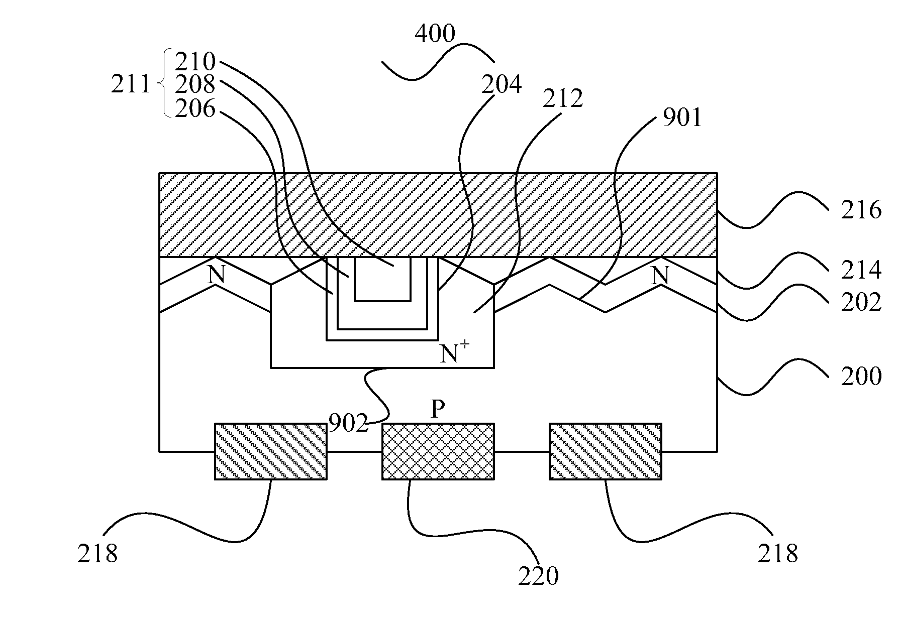
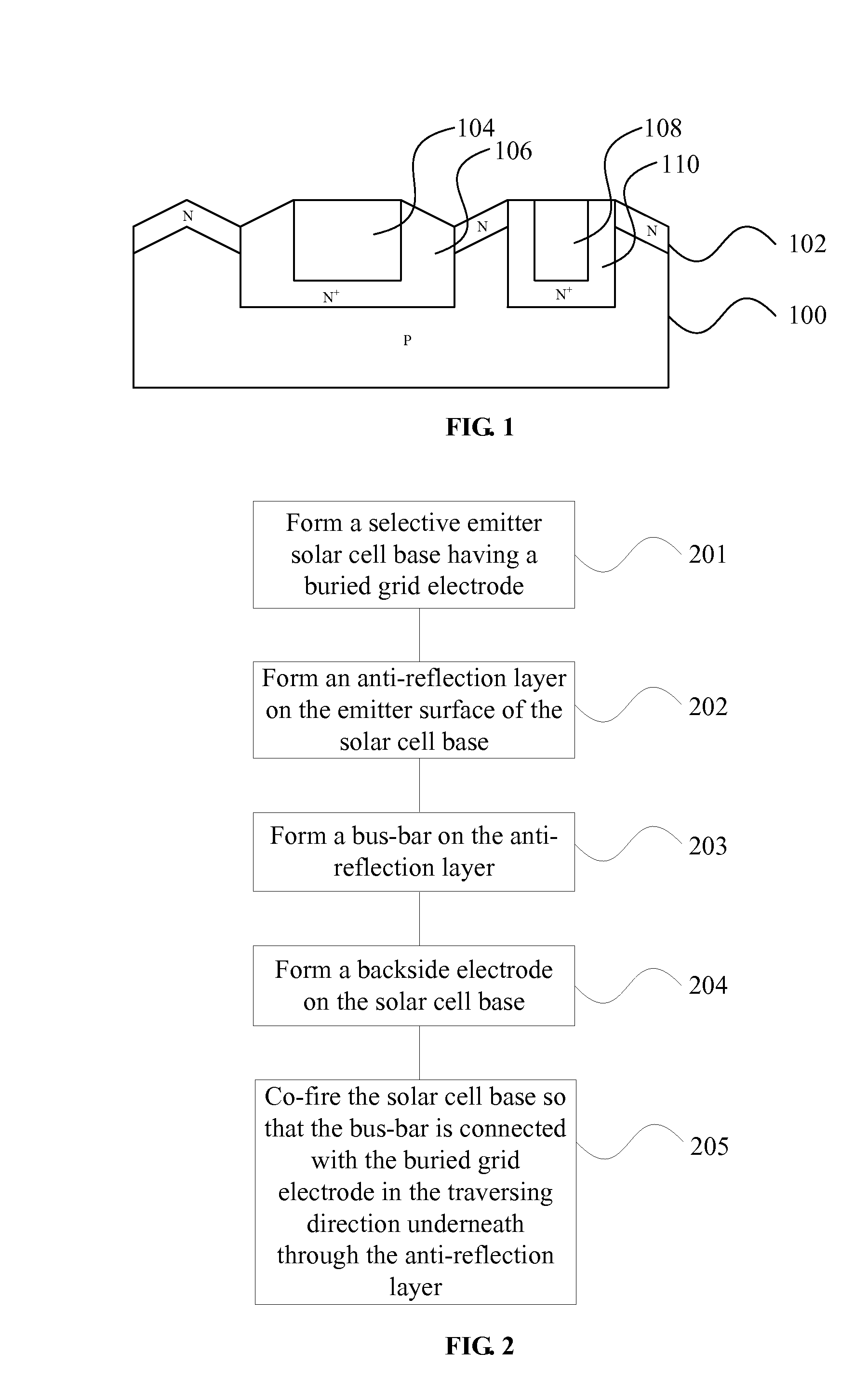
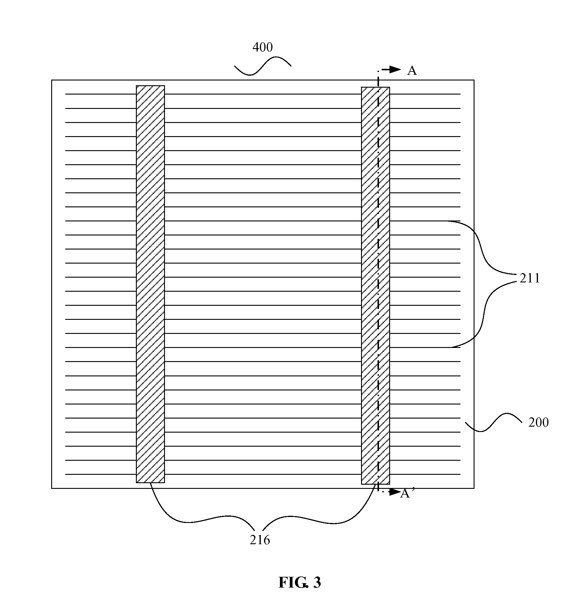
[0047]In the method for fabricating a selective emitter solar cell according to the invention, an anti-reflection layer is formed on a surface of a selective emitter solar cell base. The selective emitter solar cell base has buried grid electrodes. Bus-bars are formed on the anti-reflection layer. The Bus-bars are connected with the buried grid electrodes used as emitters in the traversing direction underneath through the anti-reflection layer. Therefore, the emitters and the bus-bars can be made separately. The width of the emitters can be reduced according to actual needs, the area that is unnecessarily taken may be reduced, the effective area for a solar cell panel to receive sunlight may be increased, the contact resistance between the emitters and emitter grooves may be reduced, which may lead to an improved conversion efficiency of the solar cell panel.

[0048]In addition, in the method for fabricating a selective emitter solar cell, a lowered doping concentration of the semicon...


PUM


Abstract

A fabrication method of a selective emitter solar cell, including: forming a selective emitter solar cell base having a buried grid electrode; forming an anti-reflection layer on the emitter surface of the solar cell base; forming a bus-bar on the anti-reflection layer; and connecting the buried grid electrode with the bus-bar in the traversing direction underneath through the anti-reflection layer. Accordingly, the invention provides a selective emitter solar cell. With the method of the invention, emitters and bus-bars are made separately, the width of the emitters can be reduced according to actual needs, the area that is unnecessarily taken may be reduced, the effective area for a solar cell panel to receive sunlight may be increased. The invention improves conversion efficiency of a selective emitter solar cell panel from 16.5% to 18% or more.

Description

FIELD OF THE INVENTION [0001]The present invention relates to the field of semiconductor manufacture, and in particular to a selective emitter solar cell and a fabrication method thereof.BACKGROUND OF THE INVENTION [0002]Due to limitations of conventional energy supplies and an increasing pressure to environmental protection, there is a trend of developing and using new energies in many countries. Among those new energies, the solar energy, as a clean, non-polluting and inexhaustible green energy, has drawn great attention and been heavily researched in most of the countries. In the world where energy deficiency is increasingly severe, the solar energy has a broad future.[0003]Using solar cells to convert solar energy into electrical energy is an important technical basis for massive utilization of solar energy. The ratio between the part of solar energy converted into electrical energy and the solar energy received by a solar cell, named conversion efficiency, is up to 29% theoreti...

Claims


Application Information

Patent Timeline
Patent Type & Authority Applications(United States)
IPC IPC(8): H01L31/00H01L31/0232H01L21/50
CPCH01L31/022425H01L31/03529Y02E10/547H01L31/1804H01L31/068Y02P70/50
Inventor LIN, JANG-SHEN
Owner SEMICONDUCTOR MANUFACTURING INTERNATIONAL (BEIJING) CORP
Why Eureka
Try Eureka