Light-emitting device and method for manufacturing the same

Active Publication Date: 2010-02-18
PANASONIC INTELLECTUAL PROPERTY MANAGEMENT CO LTD
View PDF32 Cites 86 Cited by
  • Summary
  • Abstract
  • Description
  • Claims
  • Application Information

AI Technical Summary

Benefits of technology

[0015]According to the light-emitting device of the present invention, the light guide portion made of the light-transmitting material is arranged in the wavelength converting layer, thereby preventing the light from the light-emitting element from being reflected by the wavelength converting material and reabsorbed into the light-emitting element. Further, the wavelength converting layer can be made smaller in size because there is no need to reduce the concentration of

Problems solved by technology

Thus, the efficiency of extracting white light may be decreased.
However, this makes the wavelength converting layer and, accordingly, th

Method used


Image

  • Light-emitting device and method for manufacturing the same
  • Light-emitting device and method for manufacturing the same
  • Light-emitting device and method for manufacturing the same

Examples


Example

Embodiment 1

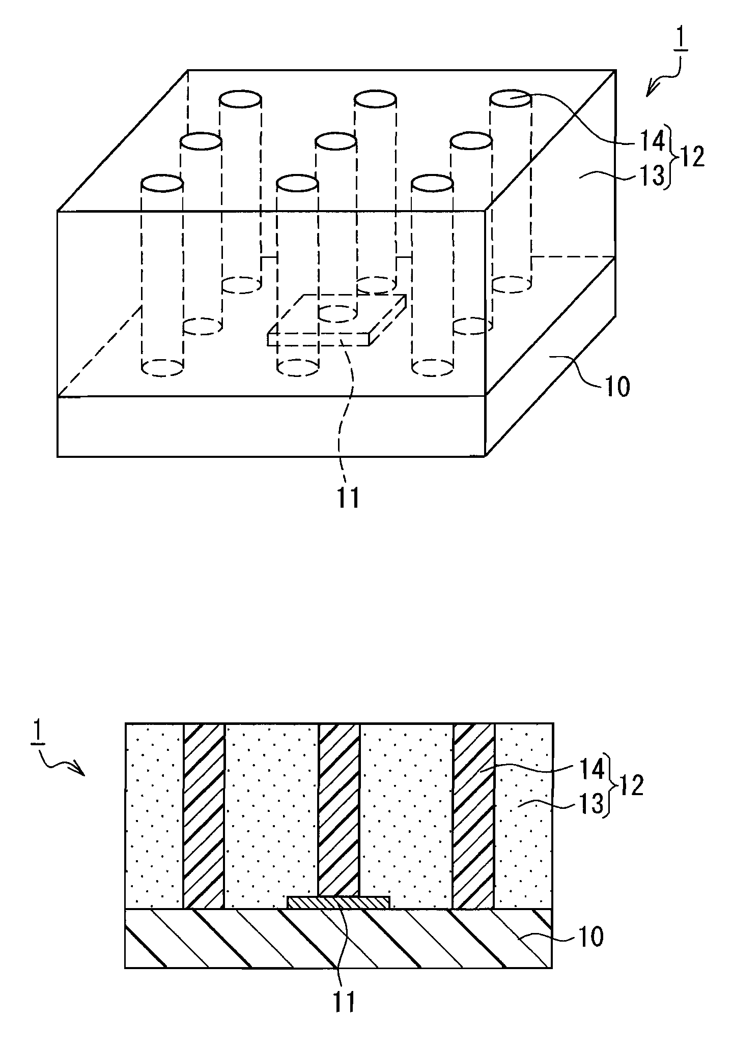
[0047]FIG. 1A is a schematic perspective view showing a light-emitting device according to Embodiment 1 of the present invention, and FIG. 1B is a schematic cross-sectional view of the light-emitting device shown in FIG. 1A.

[0048]As shown in FIGS. 1A and 1B, a light-emitting device 1 includes a base 10, a light-emitting element 11 placed on the base 10, and a wavelength converting layer 12 that covers the light-emitting element 11. The wavelength converting layer 12 includes a wavelength converting portion 13 containing a wavelength converting material for converting a wavelength of light from the light emitting element 11, and nine light guide portions 14 made of a light-transmitting material. Each of the light guide portions 14 extends from a light-emitting element 11 side to a light extraction side (top surface) of the wavelength converting layer 12. With this configuration, it is possible to prevent the light from the light-emitting element 11 from being reflected by...

Example

Embodiment 2

[0054]FIG. 3A is a schematic perspective view showing a light-emitting device according to Embodiment 2 of the present invention, and FIG. 3B is a schematic cross-sectional view of the light-emitting device shown in FIG. 3A. As shown in FIGS. 3A and 3B, in a light-emitting device 6, the wavelength converting layer 13 has a three-layer structure, in which a red phosphor layer 131, a green phosphor layer 132, and a blue phosphor layer 133 are laminated sequentially from a base 10 side. Further, an ultraviolet LED is used as the light-emitting element 11. With this configuration, it is possible to prevent a phosphor in the red phosphor layer 131 from being excited by green light from the green phosphor layer 132 and to prevent a phosphor in the red phosphor layer 131 and a phosphor in the green phosphor layer 132 from being excited by blue light from the blue phosphor layer 133. Consequently, the luminous efficiency can be improved. Further, the light guide portion 14 inclu...

Example

Embodiment 3

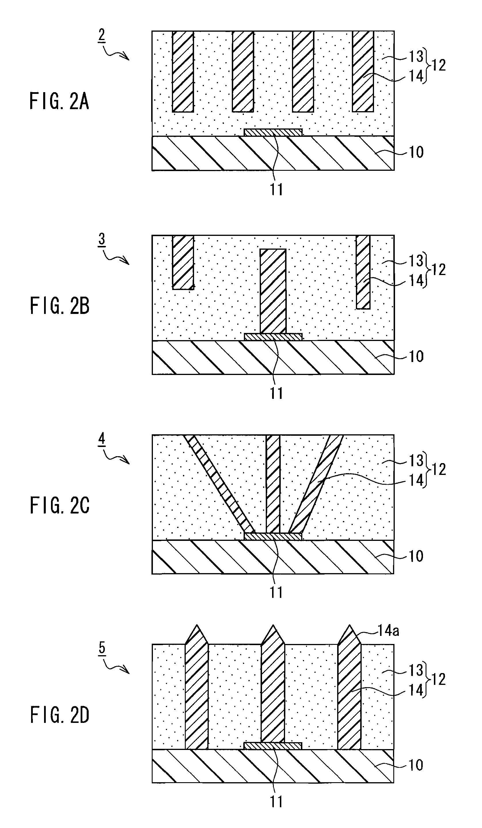
[0055]Next, a method for manufacturing a light-emitting device according to Embodiment 3 of the present invention will be described with reference to the drawings. FIGS. 4A to 4C and FIGS. 5A and 5B to be referred to are cross-sectional views showing process steps in the method for manufacturing the light-emitting device according to Embodiment 3. Note here that the method for manufacturing the light-emitting device according to Embodiment 3 is a preferred example of a method for manufacturing the above-described light-emitting device 2 (see FIG. 2A).

[0056]Initially, as shown in FIG. 4A, the light-emitting element 11 is placed on the base 10. Then, a wavelength converting material layer 20 made of a light-transmitting base material and a wavelength converting material dispersed in the light-transmitting base material is formed on the base 10 by screen printing or the like so as to cover the light-emitting element 11.

[0057]Then, as shown in FIG. 4B, a jig 21 with rod-like...


PUM


Abstract

A light-emitting device (1) includes a base (10), a light-emitting element (11) placed on the base (10), and a wavelength converting layer (12) that covers the light-emitting element (11). The wavelength converting layer (12) includes a wavelength converting portion (13) that converts a wavelength of light from the light-emitting element (11), and a light guide portion (14) made of a light-transmitting material, and the light guide portion (14) extends from a light-emitting element (11) side to a light extraction side of the wavelength converting layer (12). Consequently, it is possible to provide a light-emitting device that can be miniaturized and reduced in thickness easily and can prevent a decrease in the light extraction efficiency.

Description

TECHNICAL FIELD[0001]The present invention relates to a light-emitting device using a light-emitting element and a method for manufacturing the same.BACKGROUND ART[0002]Light-emitting elements such as a light-emitting diode (hereinafter, referred to as a “LED”) are used in various types of light-emitting devices. The LED may replace an existing light source that uses discharge and radiation, due to the recently increased luminous flux, as well as the smaller size and higher efficiency compared with those of the existing light source. Furthermore, the LED is smaller in size compared with the light source using discharge and radiation, so that the LED has advantages in the applicability to increased applications, the ease of handling, the expectation of various designs, and the like. Thus, the LED is a light source having increased added values.[0003]Furthermore, the LED is capable of controlling the radiation pattern of emitted light, in combination with an optical system having a re...

Claims


Application Information

Patent Timeline
IPC IPC(8): H01L33/00H01L33/50H01L33/54H01L33/58
CPCH01L33/508H01L33/54H01L33/58H01L2933/0091H01L2924/0002H01L2924/00
Inventor SUGIURA, KENJINAGAI, HIDEOTAMURA, TETSUSHIUEDA, KENJIOKANO, KAZUYUKI
Owner PANASONIC INTELLECTUAL PROPERTY MANAGEMENT CO LTD
Why Eureka
Try Eureka