Electrical Conductive Structure and Electrical Device

a technology of electrical conductive structure and electrical device, which is applied in the direction of transformer/inductance coil/winding/connection, magnetic/electric field screening, etc., can solve the problems of increasing the size of the electrical device as a whole, incurring additional materials and manufacturing processes, and affecting the competitiveness of the product pri

Inactive Publication Date: 2010-02-25
DELTA ELECTRONICS INC
View PDF5 Cites 0 Cited by
  • Summary
  • Abstract
  • Description
  • Claims
  • Application Information

AI Technical Summary

Benefits of technology

[0009]This invention provides a novel electrical conductive structure which, with smaller space occupation, can serve as a primary winding and / or secondary winding of an inductive component in an electrical device or as a shielding layer for obviating the EMI between individual windings.

Problems solved by technology

However, an oversized solder ball 15 increases volume and occupies more space in the electrical conductive structure 1 and consequently increases the size of the electrical device as a whole, which is in contradiction to the current tendency towards lightweight, thin and miniaturized electrical devices.
Furthermore, using soldering tin incurs additional cost of materials and the manufacturing process, which has a negative impact on competitiveness in price of the product.
However, this practice will cause increased volume and higher costs.
Therefore, efforts still have to be made in the art to provide a smaller electrical conductive structure at lower manufacturing costs.

Method used


Image

  • Electrical Conductive Structure and Electrical Device
  • Electrical Conductive Structure and Electrical Device
  • Electrical Conductive Structure and Electrical Device

Examples


Embodiment Construction

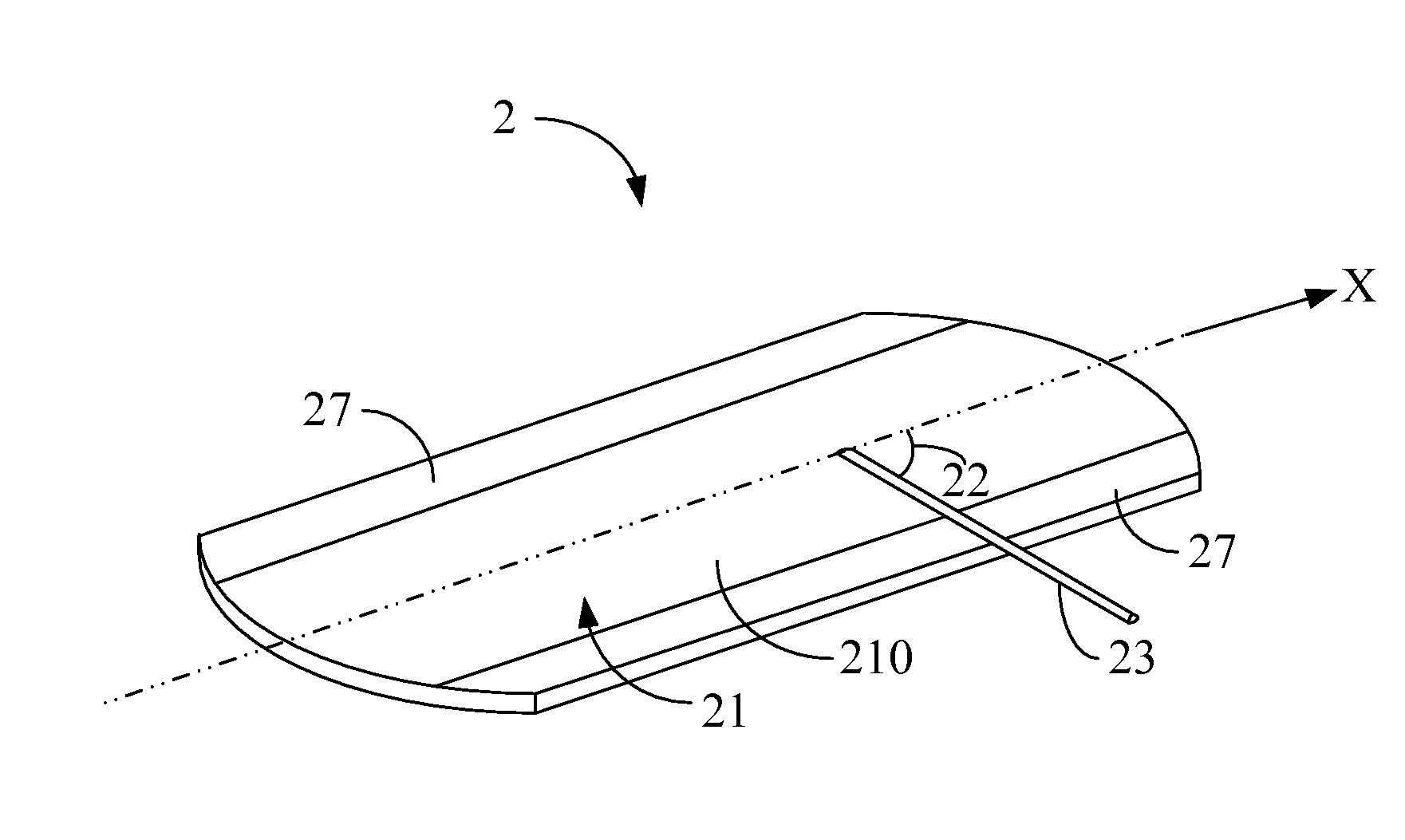
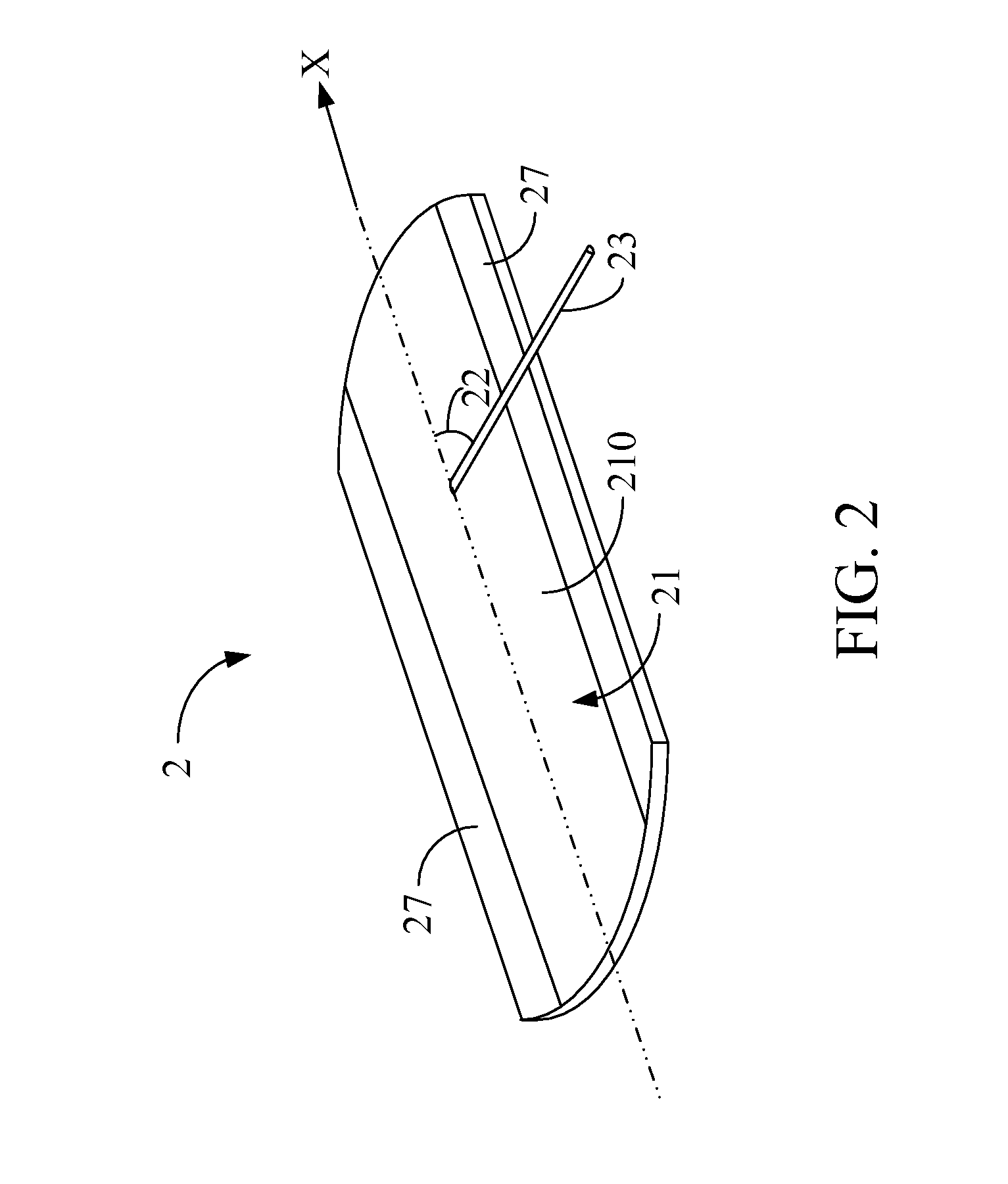
[0016]FIG. 2 depicts an embodiment of this invention, which is an electrical conductive structure 2. The electrical conductive structure 2 comprises a copper foil 21, a wire 23 and an insulating layer 27. The copper foil 21 has a first surface 210 and a second surface (not shown) opposite the first surface 210. The wire 23 is disposed adjacent to the first surface 210, while the insulating layer 27 is disposed adjacent to the second surface and folded back to cover an upper and lower portion of the first surface 210.

[0017]More specifically, the wire 23 is spot-welded on the first surface 210 of the copper foil 21 so that the copper foil 21 and the wire 23 are substantially connected with each other. The wire 23 is made of copper, e.g., enameled copper wire. However, in other embodiments, the wire 23 may also be made of other materials. It should be noticed that in other embodiments, the number of wires included in the electrical conductive structure is not limited. Also, the wire(s)...


PUM

PropertyMeasurementUnit
included angleaaaaaaaaaa
electrical conductiveaaaaaaaaaa
areaaaaaaaaaaa

Abstract

An electrical conductive structure and an electrical device comprising the electrical conductive structure are provided. The electrical conductive structure comprises a copper foil and at least one wire. The wire is disposed on the surface of the copper foil by spot welding. The electrical conductive structure is adapted to be the primary winding and/or the secondary winding of an inductive component within an electrical device as well as an electromagnetic interference (EMI) shielding between each of the winding. The electrical conductive structure of this invention combines the copper foil and at least one wire by spot welding to decrease the volume of the electrical device and to lower the costs of the assembly process.

Description

[0001]This application claims priority to Taiwan Patent Application No. 097214849 filed on Aug. 19, 2008, the disclosure of which is incorporated herein by reference in its entirety.CROSS-REFERENCES TO RELATED APPLICATIONS[0002]Not applicable.BACKGROUND OF THE INVENTION[0003]1. Field of the Invention[0004]The present invention provides an electrical conductive structure for use in electrical devices such as inductive components.[0005]2. Descriptions of the Related Art[0006]Various electrical devices that are currently available are equipped with electromagnetic inductive components that convert electric energy into magnetic energy or vice versa for filtering, energy storage or energy discharge purposes. These components help stabilize the output current. Such electromagnetic inductive components generally incorporate an electrical conductive structure which basically has two functions: to serve as a primary winding and / or a secondary winding of the electromagnetic inductive componen...

Claims


Application Information

Patent Timeline
Patent Type & Authority Applications(United States)
IPC IPC(8): H01B5/00H05K9/00
CPCH01F27/2847H01F2027/2857H01F27/362H01F27/29H01F27/36H01F27/363
Inventor LIAO, ZOLASLIANG, LF
Owner DELTA ELECTRONICS INC
Why Eureka
Try Eureka