

Enhancement mode iii-nitride device with floating gate and process for its manufacture
a technology of iiinitride and gate, which is applied in the direction of semiconductor devices, electrical devices, transistors, etc., can solve the problems of increasing cost, complicated processing steps and circuitry, and reducing device area, so as to increase reliability and reduce device area
- Summary
- Abstract
- Description
- Claims
- Application Information
AI Technical Summary
Benefits of technology
Problems solved by technology
Method used
Image

Examples
Embodiment Construction
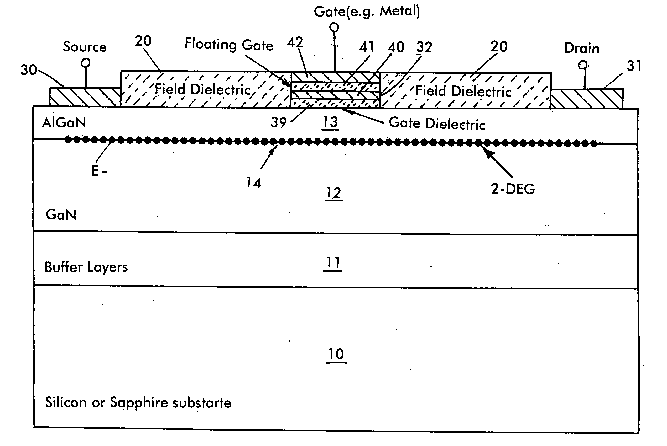
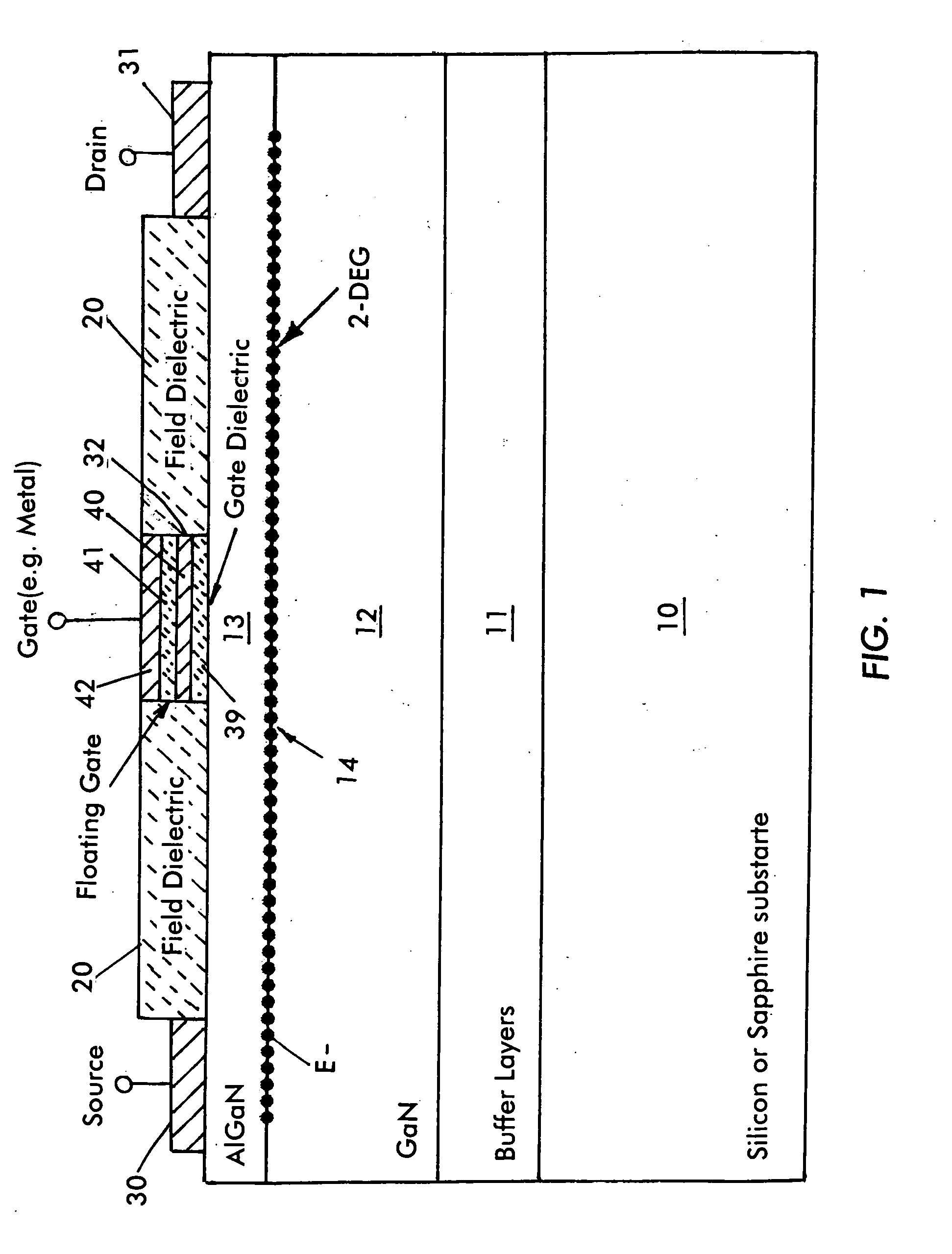
[0012]Referring first to FIG. 1, there is shown a cross-sectional view of a III-Nitride device having a floating gate, in accordance with the invention. It will be understood by those skilled in the art that the device shown may be made in wafer form in which a large number of such devices are simultaneously processed and singulated from the wafer after fabrication; and that the dimensions of the device are greatly exaggerated, for clarity.
[0013]The device of FIG. 1 is fabricated on a substrate 10 which may be silicon or sapphire or the like. Conventional buffer layers 11 are deposited atop substrate 10.
[0014]A GaN layer 12 is then conventionally deposited atop buffer layers 11 and an AlGaN layer 13 is conventionally deposited atop GaN layer.
[0015]A conductive 2-DEG layer 14 schematically represented as electrons is conventionally formed at the interface between layers 12 and 13.
[0016]The top surface of AlGaN layer 13 then receives a suitable dielectric layer 20 which can, for examp...
PUM
 Abstract
Description
Claims
Application Information