Semiconductor device
- Summary
- Abstract
- Description
- Claims
- Application Information
AI Technical Summary
Benefits of technology
Problems solved by technology
Method used
Image

Examples
first embodiment
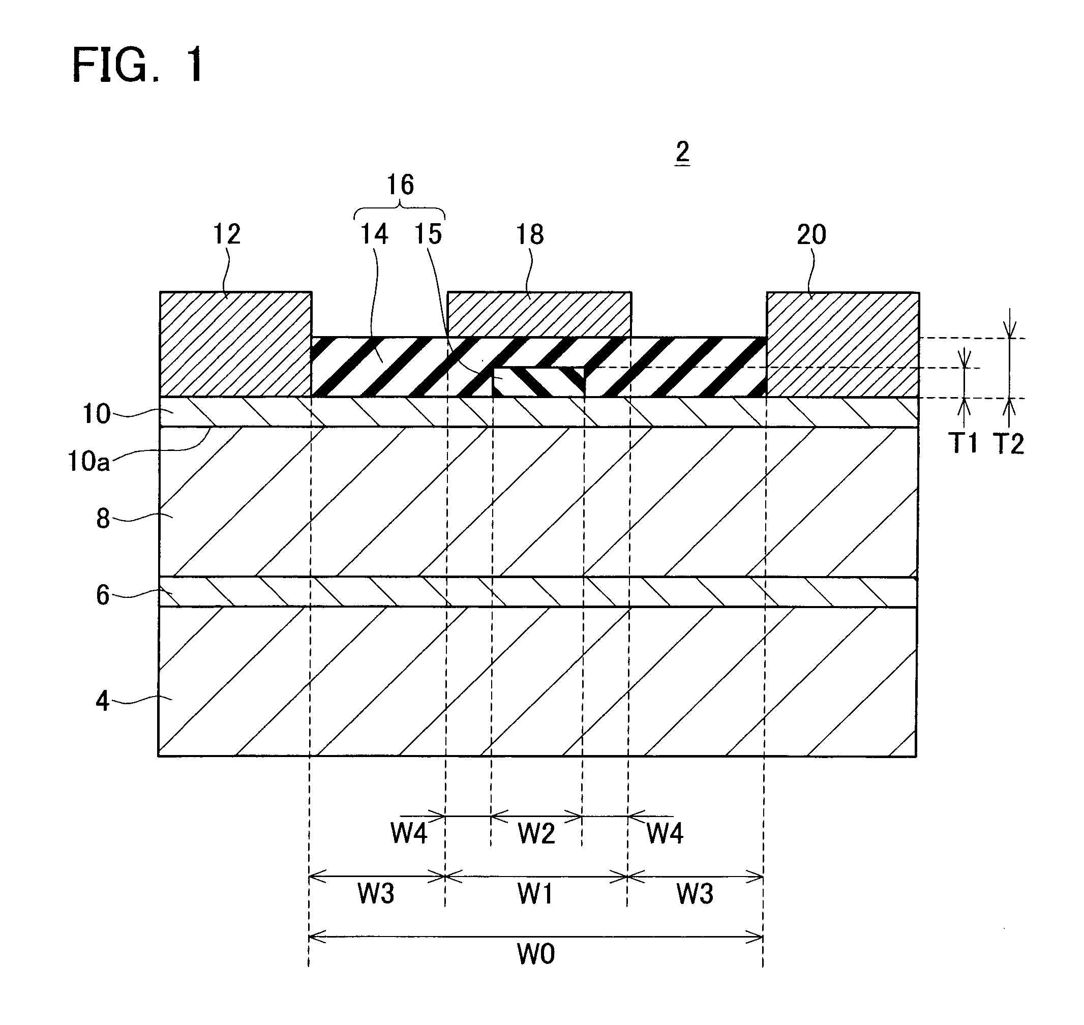
[0056]FIG. 1 is a cross-sectional view of a nitride semiconductor device 2 (which may also be referred to as a nitride based (compound) semiconductor device) according to a first embodiment of the present teachings. The nitride semiconductor device 2 is an n-channel horizontal semiconductor device having a HEMT structure. The nitride semiconductor device 2 has a sapphire substrate 4. On the surface of the sapphire substrate 4, a buffer layer 6 is stacked. The buffer layer 6 is composed of GaN. The buffer layer 6 has a thickness of 50 nm. On the surface of the buffer layer 6, a nitride semiconductor lower layer 8 is stacked. The nitride semiconductor lower layer 8 is composed of a nitride based compound; e.g. i-type GaN as in the present embodiment. As such the nitride semiconductor lower layer 8 may also be referred to as a nitride based (compound) semiconductor lower layer. The nitride semiconductor lower layer 8 has a thickness of 2 μm. On the surface of the nitride semiconductor ...
second embodiment
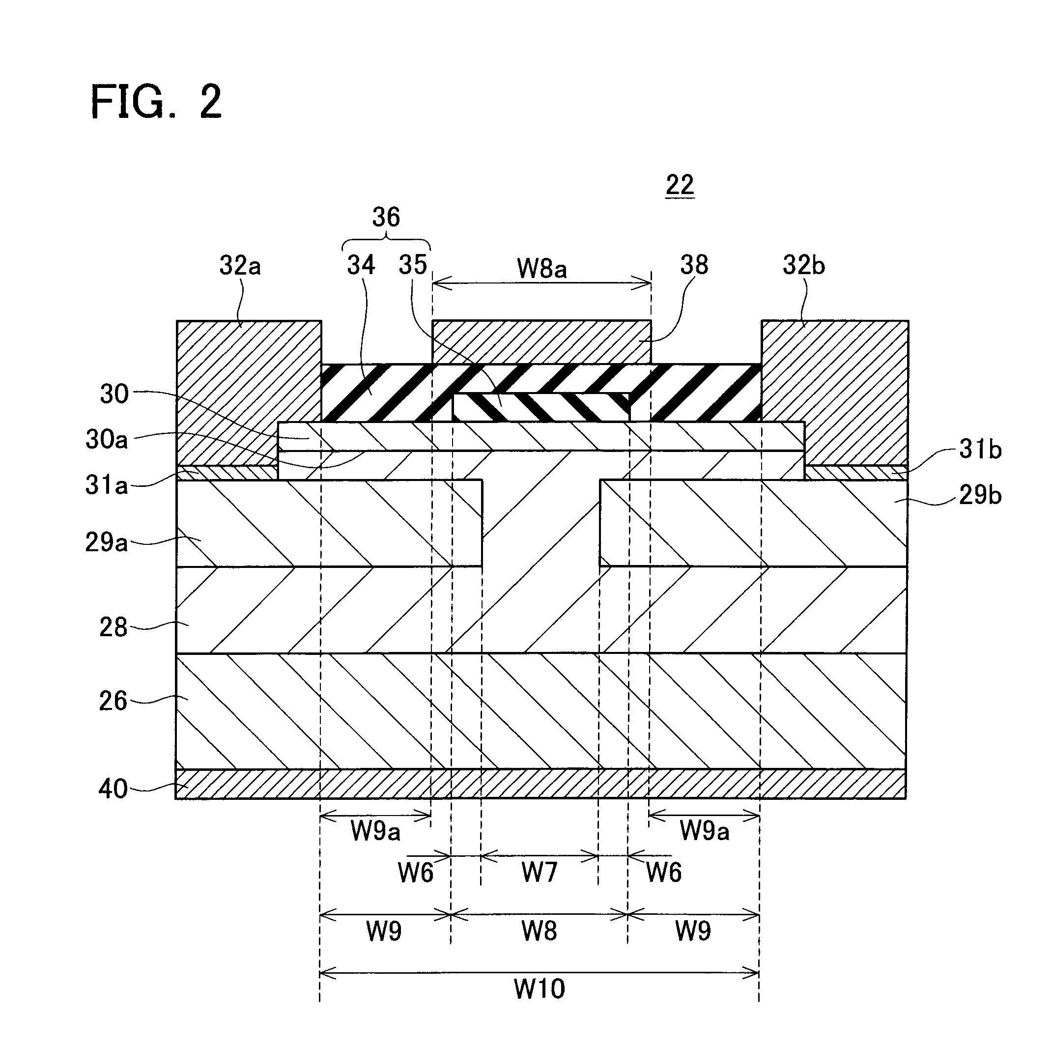
[0066]FIG. 2 is a cross-sectional view of a nitride semiconductor device 22 according to a second embodiment of the present teachings. The nitride semiconductor device 22 is an n-channel vertical semiconductor device having a HEMT structure. A drain electrode 40 is disposed on the bottom side of the device 22, a pair of source electrodes 32a and 32b is disposed on the surface side (i.e. the upper side) of the device 22, and the current flows in a vertical direction.
[0067]On the upper surface of the drain electrode 40, a nitride semiconductor substrate 26 composed of a single crystal nitride based compound is stacked. The nitride semiconductor substrate 26, which may also be referred to as a single crystal nitride based compound semiconductor substrate, is composed of n-type GaN. The nitride semiconductor substrate 26 has a thickness of 300 μm. On the surface of the nitride semiconductor substrate 26, a nitride semiconductor lower layer 28 is stacked. The nitride semiconductor lower ...
third embodiment
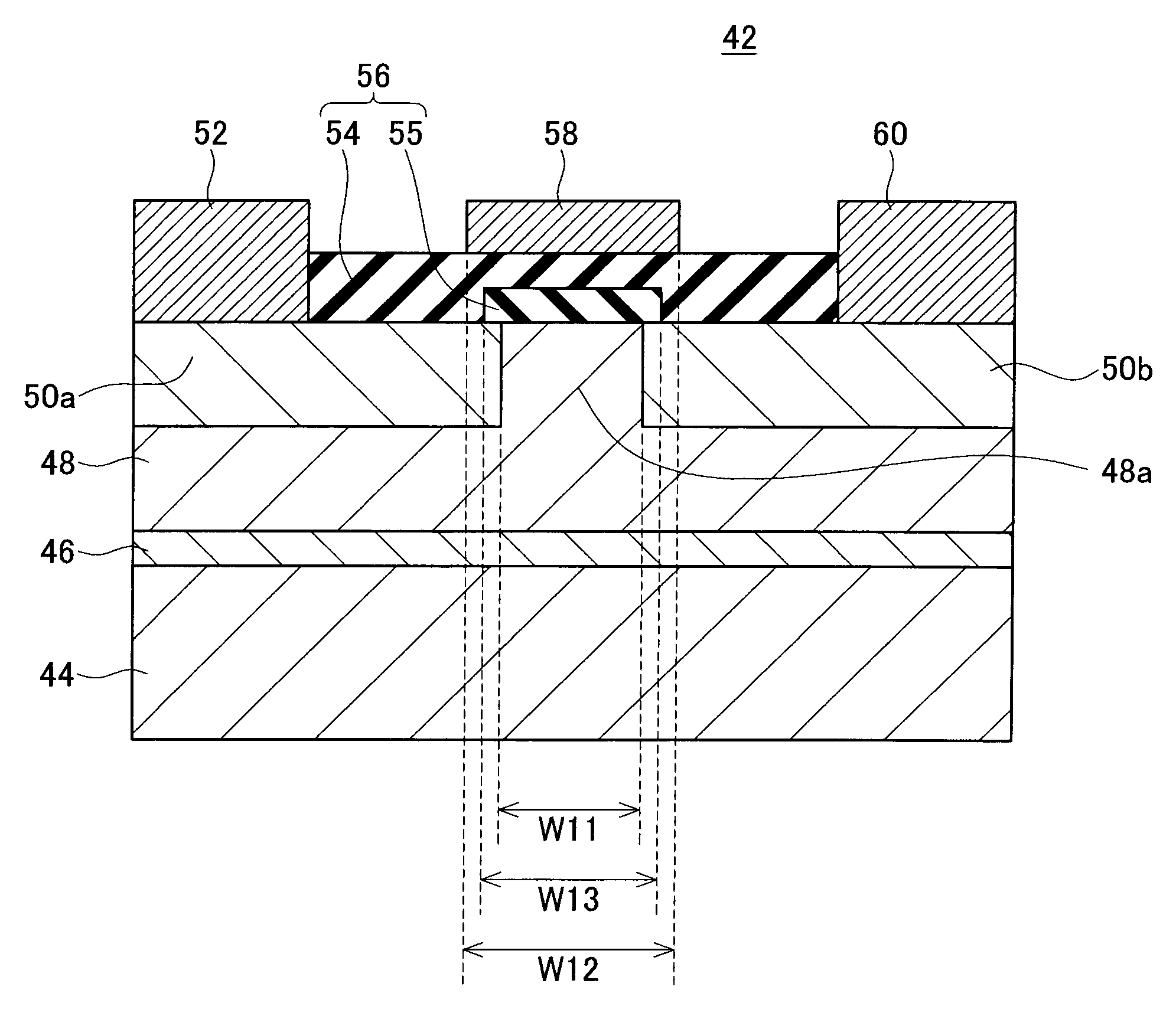
[0078]FIG. 3 is a cross-sectional view of a nitride semiconductor device 42 according to a third embodiment of the present teachings. The nitride semiconductor device 42 is an n-channel horizontal semiconductor device having a MOS structure.
[0079]The nitride semiconductor device 42 is provided with a sapphire substrate 44. On the surface of the sapphire substrate 44, a buffer layer 46 is formed. The buffer layer 46 is composed of GaN. On the surface of the buffer layer 46, a nitride semiconductor layer 48 is formed. The nitride semiconductor layer 48 is composed of p-type GaN. Within the surface of the nitride semiconductor layer 48, a protrusion portion 48a is formed. In the region on the surface of the nitride semiconductor layer 48 except for the region where the protrusion portion 48a is formed, high impurity concentration regions 50a and 50b are formed. The high impurity concentration regions 50a and 50b are composed of n+-type GaN. The high impurity concentration regions 50a a...
PUM
 Abstract
Description
Claims
Application Information
 - R&D
- Intellectual Property
- Life Sciences
- Materials
- Tech Scout
- Unparalleled Data Quality
- Higher Quality Content
- 60% Fewer Hallucinations
Browse by: Latest US Patents, China's latest patents, Technical Efficacy Thesaurus, Application Domain, Technology Topic, Popular Technical Reports.
© 2025 PatSnap. All rights reserved.Legal|Privacy policy|Modern Slavery Act Transparency Statement|Sitemap|About US| Contact US: help@patsnap.com