Semiconductor device
a technology of superjunction and semiconductor, applied in the direction of semiconductor devices, basic electric elements, electrical appliances, etc., can solve the problems of restricted drain current path and increased resistance, and achieve the effect of efficiently improving the breakdown voltag
- Summary
- Abstract
- Description
- Claims
- Application Information
AI Technical Summary
Benefits of technology
Problems solved by technology
Method used
Image

Examples
Embodiment Construction
[0025]The invention will be now described herein with reference to illustrative embodiments. Those skilled in the art will recognize that many alternative embodiments can be accomplished using the teachings of the present invention and that the invention is not limited to the embodiments illustrated for explanatory purposes.
[0026]The following is a description of an embodiment of the present invention, with reference to the accompanying drawings. In the drawings, like components are denoted by like reference numerals, and explanation of them will not be repeated.
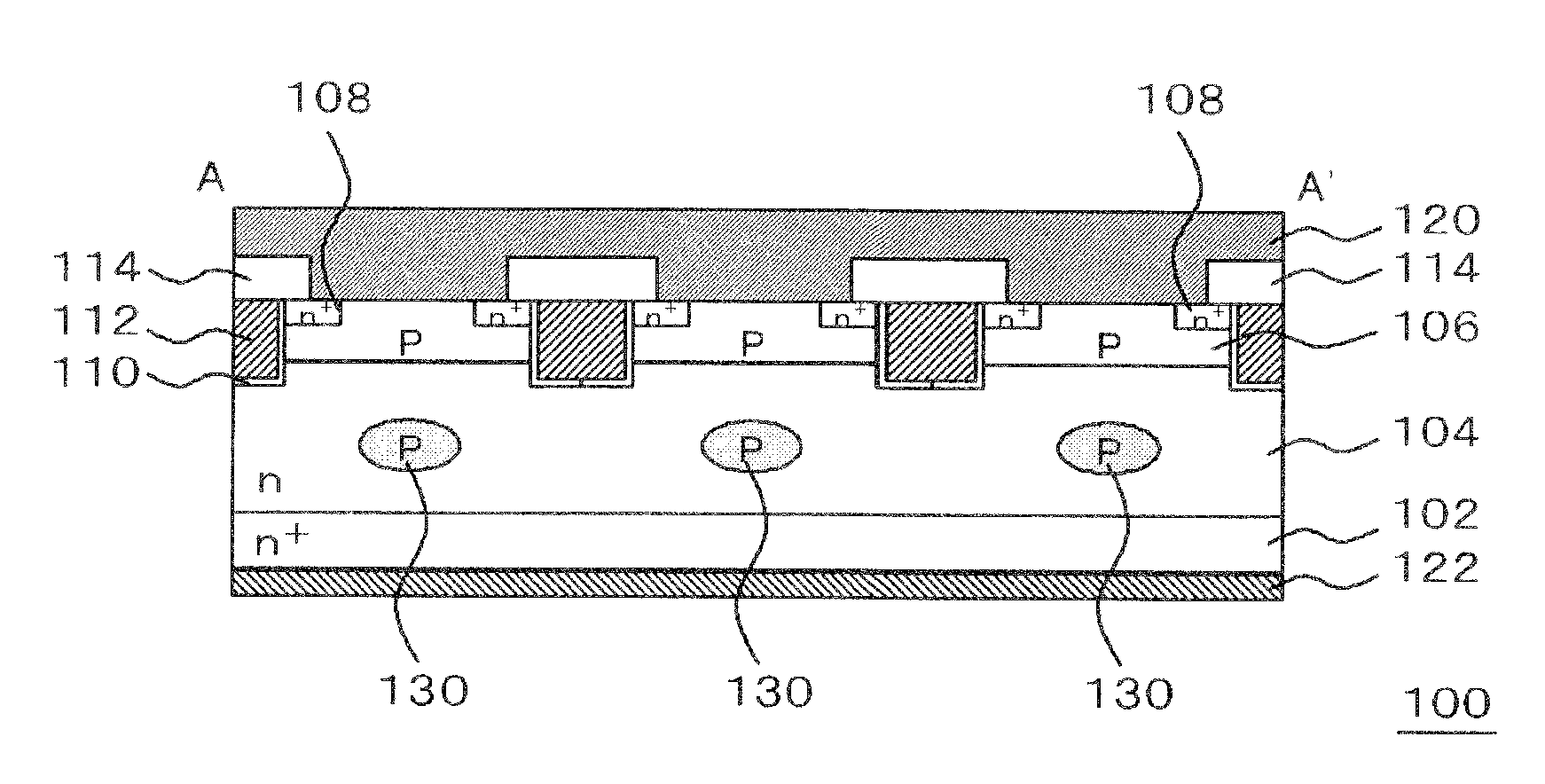
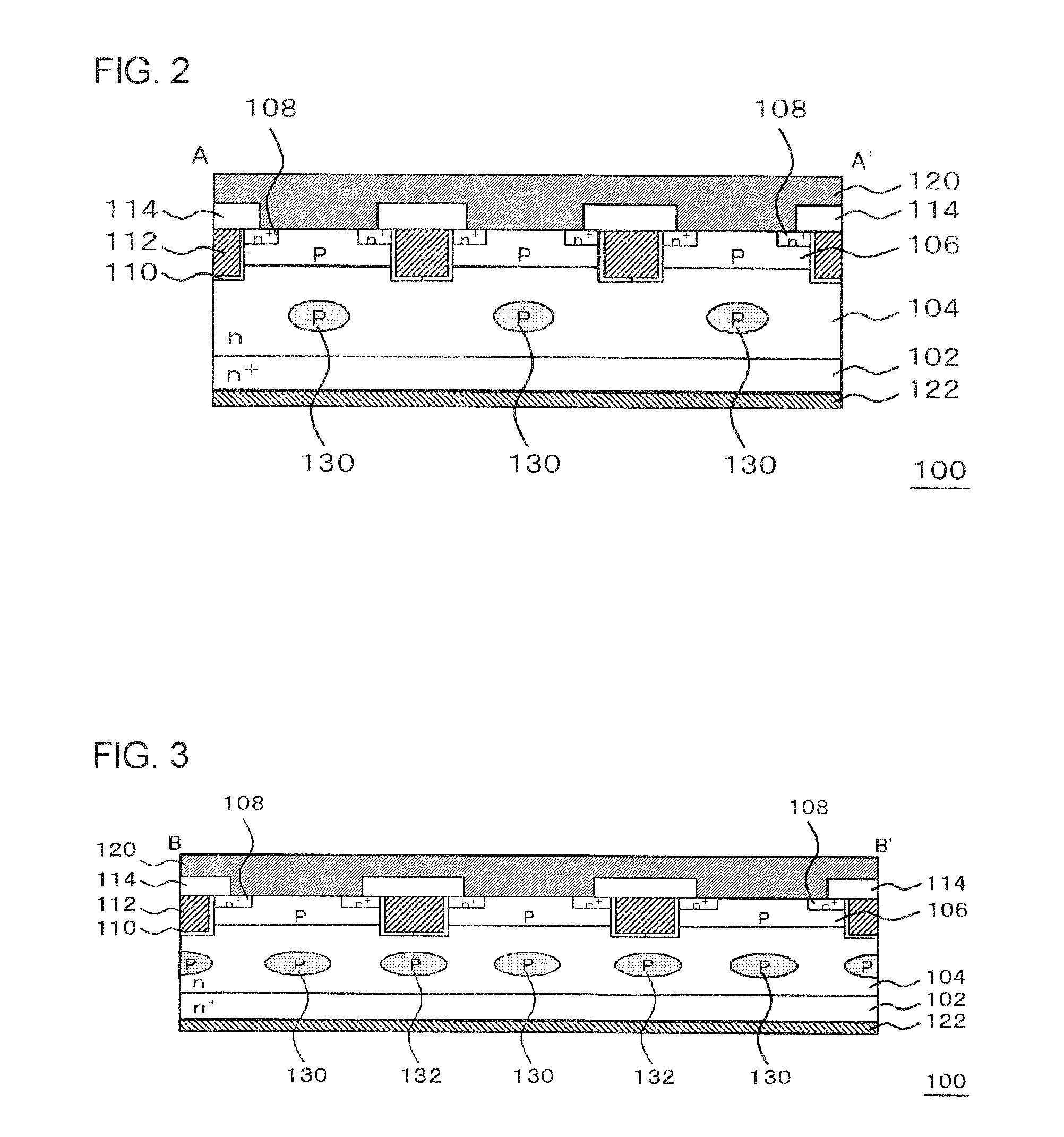
[0027]The semiconductor device of this embodiment to be described below is a MOS field effect transistor (MOSFET) having a super-junction structure. The semiconductor device may be any other vertical power device such as an insulated gate bipolar transistor (IGBT) having a super-junction structure.
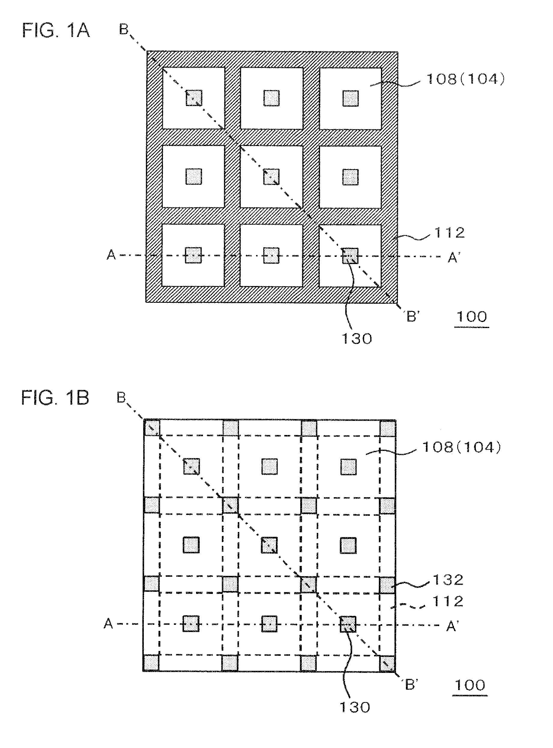
[0028]FIGS. 1A and 1B are plan views showing the structure of the MOSFET in this embodiment. To facilitate understanding of this ...
PUM
 Abstract
Description
Claims
Application Information
 - Generate Ideas
- Intellectual Property
- Life Sciences
- Materials
- Tech Scout
- Unparalleled Data Quality
- Higher Quality Content
- 60% Fewer Hallucinations
Browse by: Latest US Patents, China's latest patents, Technical Efficacy Thesaurus, Application Domain, Technology Topic, Popular Technical Reports.
© 2025 PatSnap. All rights reserved.Legal|Privacy policy|Modern Slavery Act Transparency Statement|Sitemap|About US| Contact US: help@patsnap.com