Resonant frequency device
a frequency device and resonance technology, applied in the field of resonance frequency devices, can solve the problems of limitations of the ability to fully adjust the duty cycle of modulation signals, and failure of modulation transformers and audio amplifiers, so as to improve the effect of therapeutic ionizing radiation, improve the effect of radiation on cancer cells, and improve the effect of radiation
- Summary
- Abstract
- Description
- Claims
- Application Information
AI Technical Summary
Benefits of technology
Problems solved by technology
Method used
Image
Examples
second embodiment
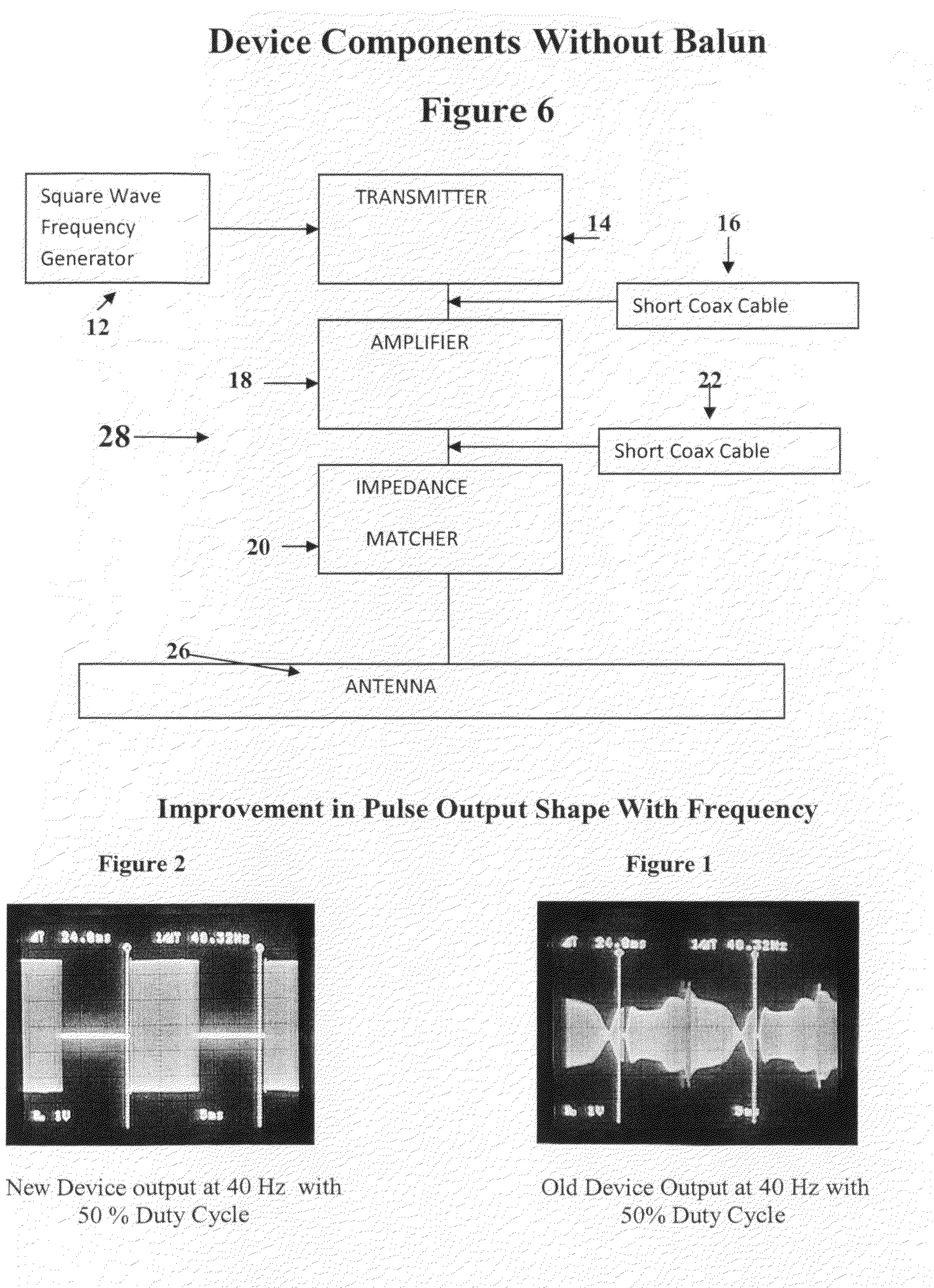
[0083]The pulse shaped, frequency response and irregularity of each carrier oscillation in the pulse is corrected by stabilizing the pulse shape at high frequencies. This is accomplished utilizing the large capacitors 78, 80 and 82 of FIG. 6 as well as the large capacitors 78, 80 and 84 of the circuit illustrated with respect to FIG. 13. It has been found that electrolytic capacitors having a range of 3300 uf to approximately 10,000 uf are added to improve the pulse shape and frequency response. The capacitor 78 in both circuits is provided in parallel to the low voltage input 70 of the power supply that powers an oscillator circuit 86. A second large electrolytic capacitor 30 having the same parameters of the capacitor 78 is provided in parallel to the high voltage input side of the circuit between the power supply 70 and the rare earth magnet 68. The large capacitor 84 of FIG. 13 is provided between the power supply 70 and the rare earth magnet 68 through a switching transistor 88...
first embodiment
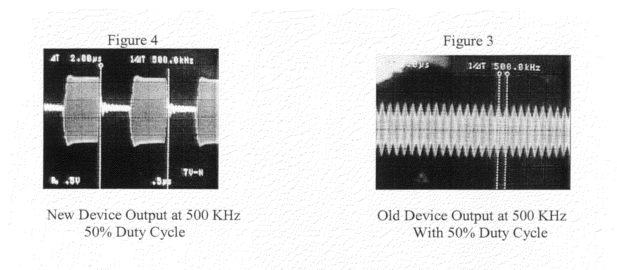
[0091]Circuit ringing between pulses can become evident at modulation frequencies of 1 MHz and above. This is important since the range of the transmitter of the present invention can be as great as 4 MHz and above. If severe enough, the circuit ringing can cause limitation of the pulse bandwidth capability. One manner in which this situation can be alleviated would be to utilize a harmonic suppressor 90 with a switching transistor 92 in the first embodiment illustrated with respect to FIG. 12. The switching transistor 92 is utilized with a resistor and a diode. The resistor is approximately 12 ohms and one end is connected to the base of the switching transistor 62. The other end of the resistor is attached to the anode of the diode. The cathode of the diode is connected to the collector of the switching transistor.
[0092]Another manner of controlling the circuit ringing is to use a switched snubber circuit 94 as illustrated in FIG. 12. The snubber circuit can be used with both the ...
PUM
 Abstract
Description
Claims
Application Information


