

Layered semiconductor light emitting device and image forming apparatus
a light emitting device and light-emitting device technology, applied in the direction of semiconductor devices, electrical equipment, basic electric elements, etc., can solve the problems of low light-output efficiency and reliability of organic el display systems, increase the size of single-crystal led systems with the number of pixels, and reduce light leakage. , the effect of enhancing light-output efficiency
- Summary
- Abstract
- Description
- Claims
- Application Information
AI Technical Summary
Benefits of technology
Problems solved by technology
Method used
Image

Examples
embodiment 1
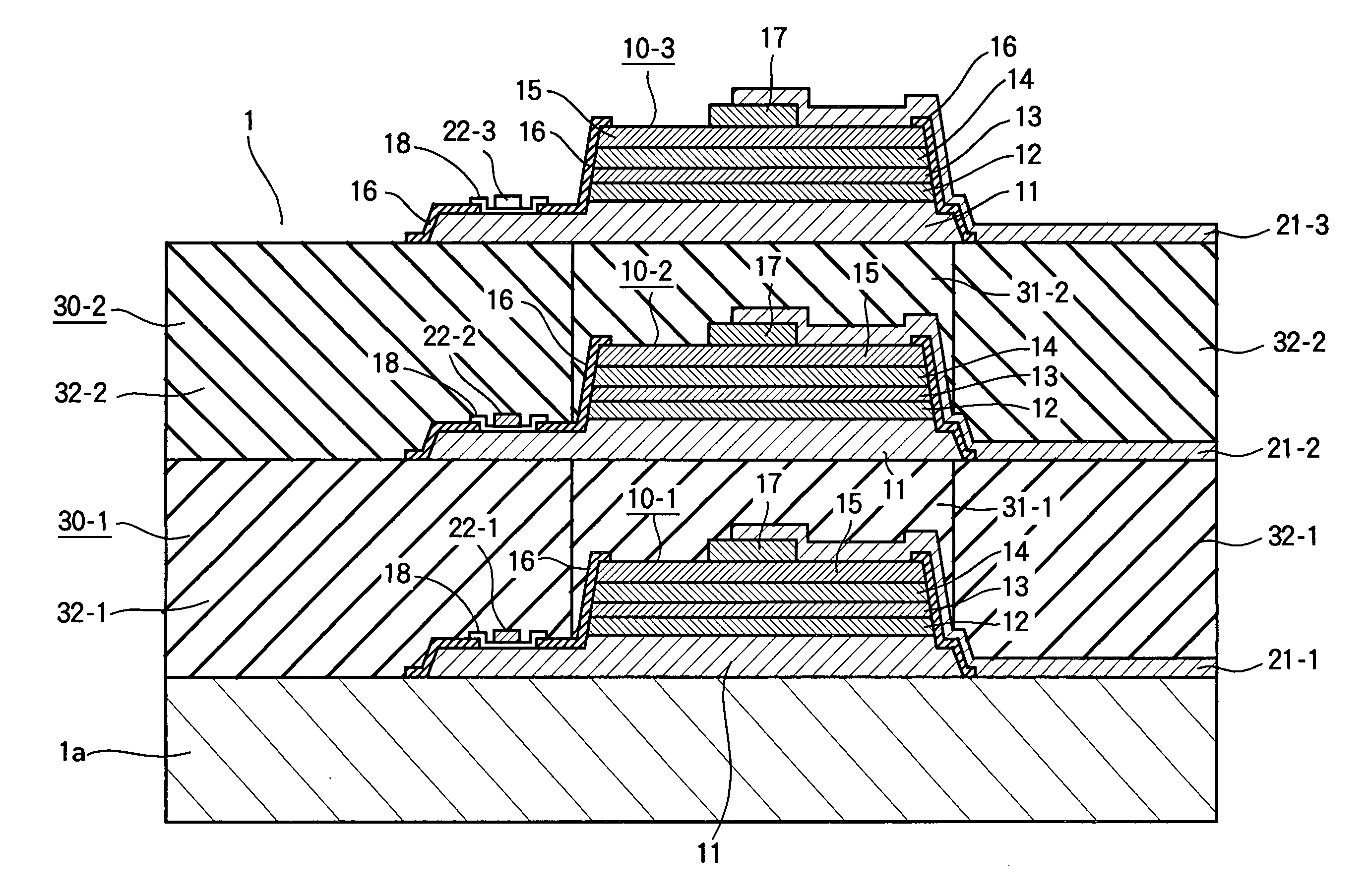
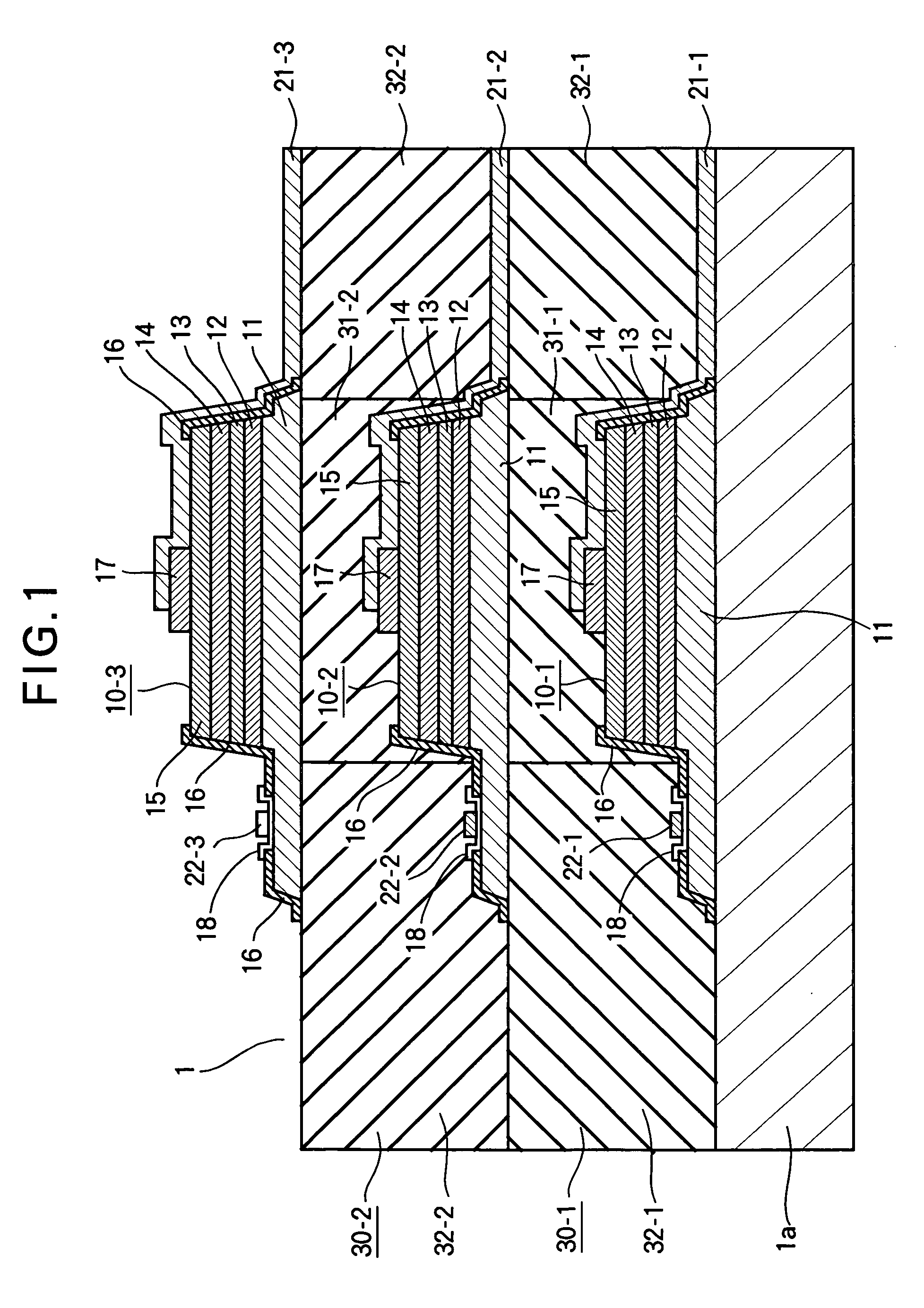
[0027]FIG. 1 is an enlarged sectional view showing a layered semiconductor light emitting device according to Embodiment 1 of the present invention, taken along line I-I in FIG. 2. FIG. 2 is a plan view showing the layered semiconductor light emitting device according to Embodiment 1 of the present invention. The layered semiconductor light emitting device (i.e., a color layered semiconductor light emitting device) includes a plurality of (for example, three) light emitting elements layered in a direction perpendicular to a light emitting surface.
[0028]The layered semiconductor light emitting device 1 of Embodiment 1 is configured to emit light upward, and has a display surface on an upper side in FIG. 1. The layered semiconductor light emitting device 1 includes a supporting substrate 1a on which a first-layer semiconductor light emitting element 10-1 is formed. The first-layer semiconductor light emitting element 10-1 can be preliminarily formed on a base material, be separated fr...
embodiment 2
[0068]FIG. 4 is an enlarged plan view showing a layered semiconductor light emitting device according to Embodiment 2 of the present invention. FIG. 5 is a sectional view taken along line V-V in FIG. 4. In FIGS. 4 and 5, components that are the same as those of Embodiment 1 (FIGS. 1 and 2) are assigned the same reference numerals. In FIGS. 4 and 5, the layered semiconductor light emitting device (i.e., a color layered semiconductor light emitting device) 1A includes a plurality of (for example, three) light emitting elements layered in a direction perpendicular to a light emitting surface as in Embodiment 1.
[0069]The layered semiconductor light emitting device 1A of Embodiment 2 includes a first-layer planarizing layer 30-1A and a second-layer planarizing layer 30-2A instead of the first-layer planarizing layer 30-1 and the second-layer planarizing layer 30-2 of Embodiment 1 (FIG. 2). The first-layer planarizing layer 30-1A and the second-layer planarizing layer 30-2A respectively h...
embodiment 3
[0078]FIG. 6 is a plan view showing an image forming apparatus according to Embodiment 3 of the present invention. The image forming apparatus according to Embodiment 3 includes the layered semiconductor light emitting device 1 of Embodiment 1 or the layered semiconductor light emitting device 1A of Embodiment 2.
[0079]The image forming apparatus according to Embodiment 3 is configured so that, for example, the layered semiconductor light emitting devices 1 of Embodiment 1 or the layered semiconductor light emitting devices 1A of Embodiment 2 are two-dimensionally arranged on the supporting substrate 1a. All of the layered semiconductor light emitting devices 1 (or the layered semiconductor light emitting devices 1A) are electrically connected to each other via the upper electrode common wirings 23-1, 23-2 and 23-3 and the lower electrode 24. The upper electrode common wirings 23-1, 23-2 and 23-3 and the lower electrodes 24 extend to the vicinity of the outer edge of the supporting s...
PUM
 Abstract
Description
Claims
Application Information