Pixel circuit, light emitting display device and driving method thereof

a light-emitting display device and pixel circuit technology, applied in the field of pixels, can solve the problems of large line load, difficult application of current-writing type pixel circuit to a large-screen display, and long writing time, and achieve the effect of high-quality display

Inactive Publication Date: 2010-03-04
CANON KK
View PDF12 Cites 64 Cited by
  • Summary
  • Abstract
  • Description
  • Claims
  • Application Information

AI Technical Summary

Benefits of technology

[0029]According to the present invention, a light emitting display device with a large line load, for example, a large screen OLED display, which enables high quality display with a threshold voltage and mobility being corrected by writing a current from outside can be realized.

Problems solved by technology

However, in the case of a current-writing type pixel circuit, a line load on the display is charged and discharged with a current, and therefore, much time is taken for writing.
Accordingly, the current-writing type pixel circuit is difficult to be applied to a large screen display, because as the display size is larger, the line load becomes larger.
Further, especially in a large screen display, writing of current takes much time, and application of a current-writing type pixel circuit with high precision is difficult.

Method used


Image

  • Pixel circuit, light emitting display device and driving method thereof
  • Pixel circuit, light emitting display device and driving method thereof
  • Pixel circuit, light emitting display device and driving method thereof

Examples


embodiment 1

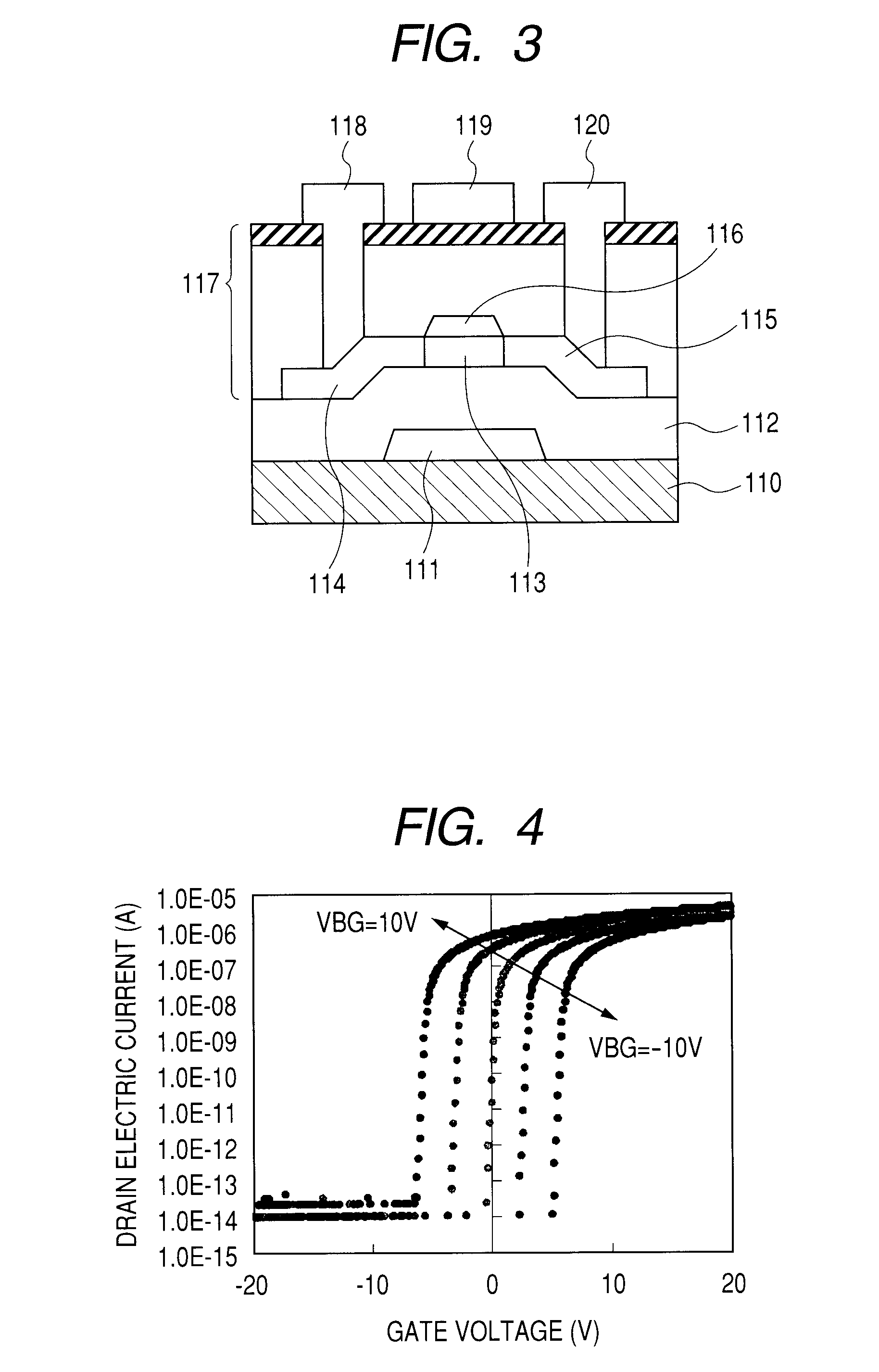
[0058]First, the characteristics of a TFT having a back gate electrode and has a-IGZO as a channel layer, which is used in the present embodiment, will be described.

[0059]FIG. 3 is a sectional view of TFT having a back gate electrode and a-IGZO as a channel layer.

[0060]A production method of a-IGZO TFT having a structure illustrated in FIG. 3 will be described hereinafter.

[0061]A Mo film (100 nm thick) is deposited on a glass substrate 110 which is an insulating substrate by a sputtering deposition method, and by a photolithography method and dry etching, a gate electrode 111 is formed.

[0062]Thereafter, by a plasma CVD deposition method, an SiO film (200 nm thick) is deposited, and a gate insulating layer 112 is formed.

[0063]Thereafter, at a room temperature, by a sputtering deposition method, an a-IGZO film (30 nm thick) is deposited, and is islanded by a photolithography method and wet etching. The a-IGZO film functions as part of a channel region (channel layer) 113 ...

embodiment 2

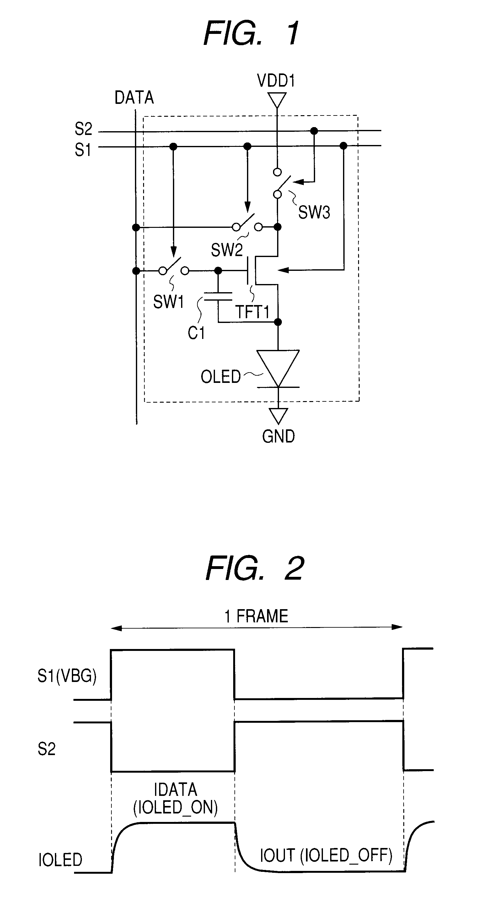
[0100]FIG. 7 illustrates a pixel circuit of an OLED display of embodiment 2. As illustrated in FIG. 7, in this embodiment, the switch SW3 and the scanning line S2 are removed from embodiment 1, connection of the switch SW1 is changed to between the gate and drain of the TFT 1, and connection of the switch SW2 is switched to between the source and data lines of the TFT 1.

[0101]An operation thereof will be described hereinafter.

[0102](a) Current Writing Period

[0103]In the current writing period, a current (IDATA) supplied from outside the pixel circuit through the data line DATA is written to the TFT 1.

[0104]In the current writing period, the voltage of the scanning line S1 is set to an H level (VH). Accordingly, the switches SW1 and SW2 are in an electrically continuing (ON) state. Further, the back gate voltage of the TFT 1 becomes VH, and the current capability is in a high state. Further, the level of the power supply line VDD 1 is set to be the threshold voltage of the OLED eleme...

embodiment 3

[0114]A pixel circuit of an OLED display of embodiment 3 is illustrated in FIG. 8. The characteristic of the present embodiment is that the voltage change between the back gate and source omitted in embodiments 1 and 2 are made correctable. Thereby, change and variation of the threshold voltage of the OLED element can be corrected.

[0115]As illustrated in FIG. 8, in this embodiment, a capacitor C2, the switch SW3, a switch SW4, a switch SW5, a scanning line S2, a scanning line S3, a reference voltage line VR1 and a reference voltage line VR2 are added as compared with the configuration of embodiment 2 illustrated in FIG. 7. The capacitor C2 is disposed between the back gate and source of the TFT 1. The switch SW3 is disposed between the back gate of the TFT 1 and the reference voltage line VR1, the switch SW4 is disposed between the source of the TFT1 and the reference voltage line VR2, and the switch SW5 is disposed between the source of the TFT 1 and the anode of the OLED. The scan...


PUM


Abstract

A pixel circuit including at least a light emitting element, and a thin film transistor that supplies to the light emitting element a first current controlling a gray scale according to luminance-current characteristics of the light emitting element, wherein the thin film transistor has a back gate electrode, at least a driving period in which the thin film transistor supplies the first current to the light emitting element, and a writing period in which a second current is written to the thin film transistor before the driving period in order to pass the first current to the thin film transistor during the driving period are included, and by changing voltages which are applied to the back gate electrode in the driving period and the writing period, current capability to a gate voltage of the thin film transistor is made to differ.

Description

BACKGROUND OF THE INVENTION[0001]1. Field of the Invention[0002]The present invention relates to a pixel circuit using a light emitting display device element, a light emitting display device and a driving method thereof. The present invention particularly relates to a pixel circuit configured by an organic light emitting diode (Organic Light Emitting Diode, hereinafter called OLED) element and a drive circuit for supplying a current to the OLED element, a light emitting display device including the pixel circuits in a matrix form and a driving method thereof.[0003]2. Description of the Related Art[0004]In recent years, the research and development of OLED displays using organic light emitting diodes (OLED) as light emitting elements has been underway. In the OLED displays, an active-matrix (Active-Matrix, hereinafter called AM) type OLED display configured by pixel circuits including OLED elements and pixel circuits including circuits for driving the OLED elements is commonly used....

Claims


Application Information

Patent Timeline
Patent Type & Authority Applications(United States)
IPC IPC(8): G09G3/30H04N5/222
CPCG09G3/325G09G2300/0426G09G2300/0439G09G2320/0223G09G2300/0852G09G2310/0251G09G2310/0262G09G2300/0814G09G3/3233
Inventor ABE, KATSUMITAKAHASHI, KENJIHAYASHI, RYOKUMOMI, HIDEYA
Owner CANON KK
Why Eureka
Try Eureka