

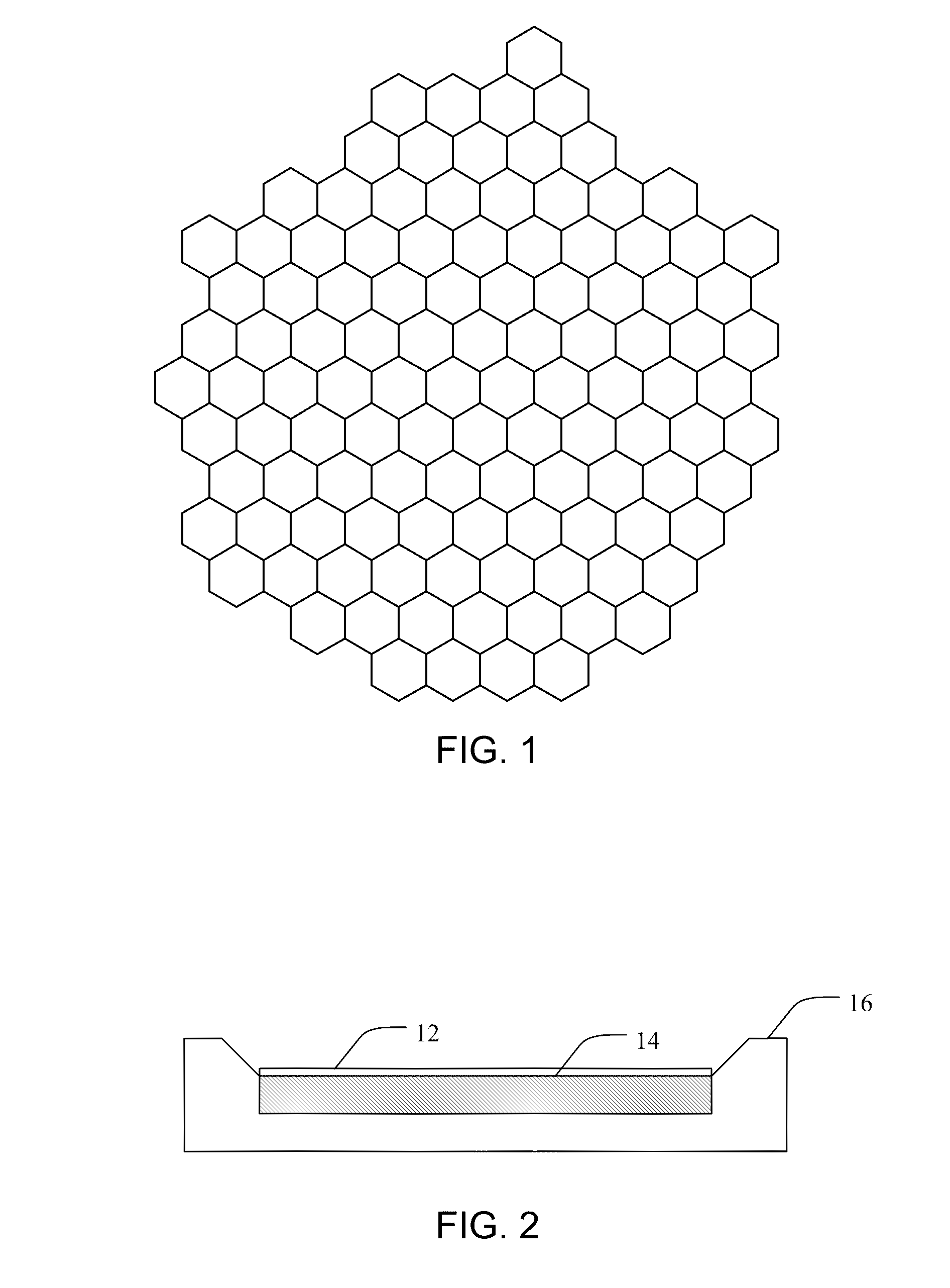
Graphene and Hexagonal Boron Nitride Planes and Associated Methods
a hexagonal boron nitride and plane technology, applied in the direction of conductors, physical/chemical process catalysts, semiconductor/solid-state device details, etc., can solve the problems of unstable curved structure formation, soot, nanotubes, and planar graphene itself being presumed to not exist in the free sta
- Summary
- Abstract
- Description
- Claims
- Application Information
AI Technical Summary
Benefits of technology
Problems solved by technology
Method used
Image

Examples
example
Example 1
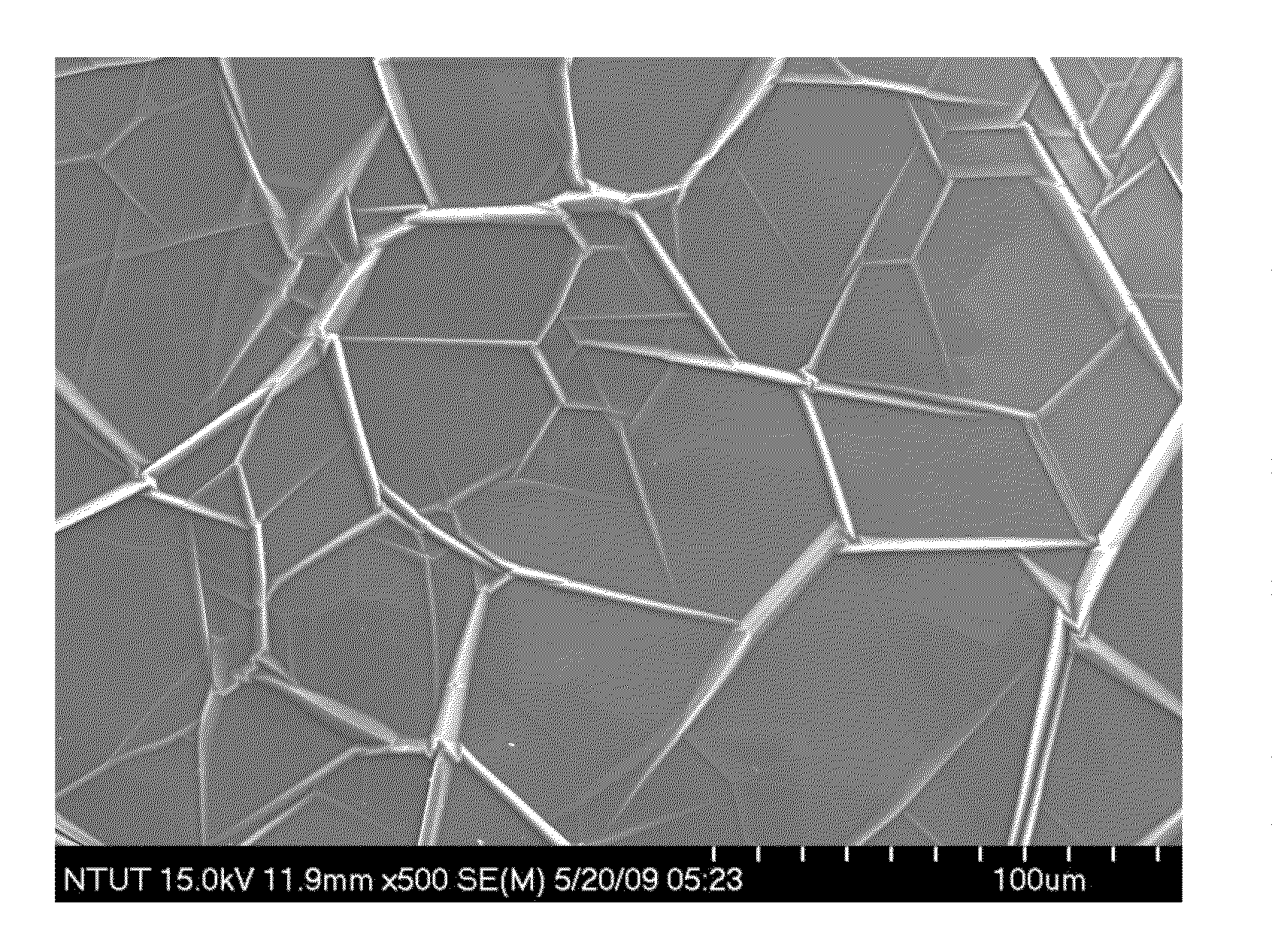
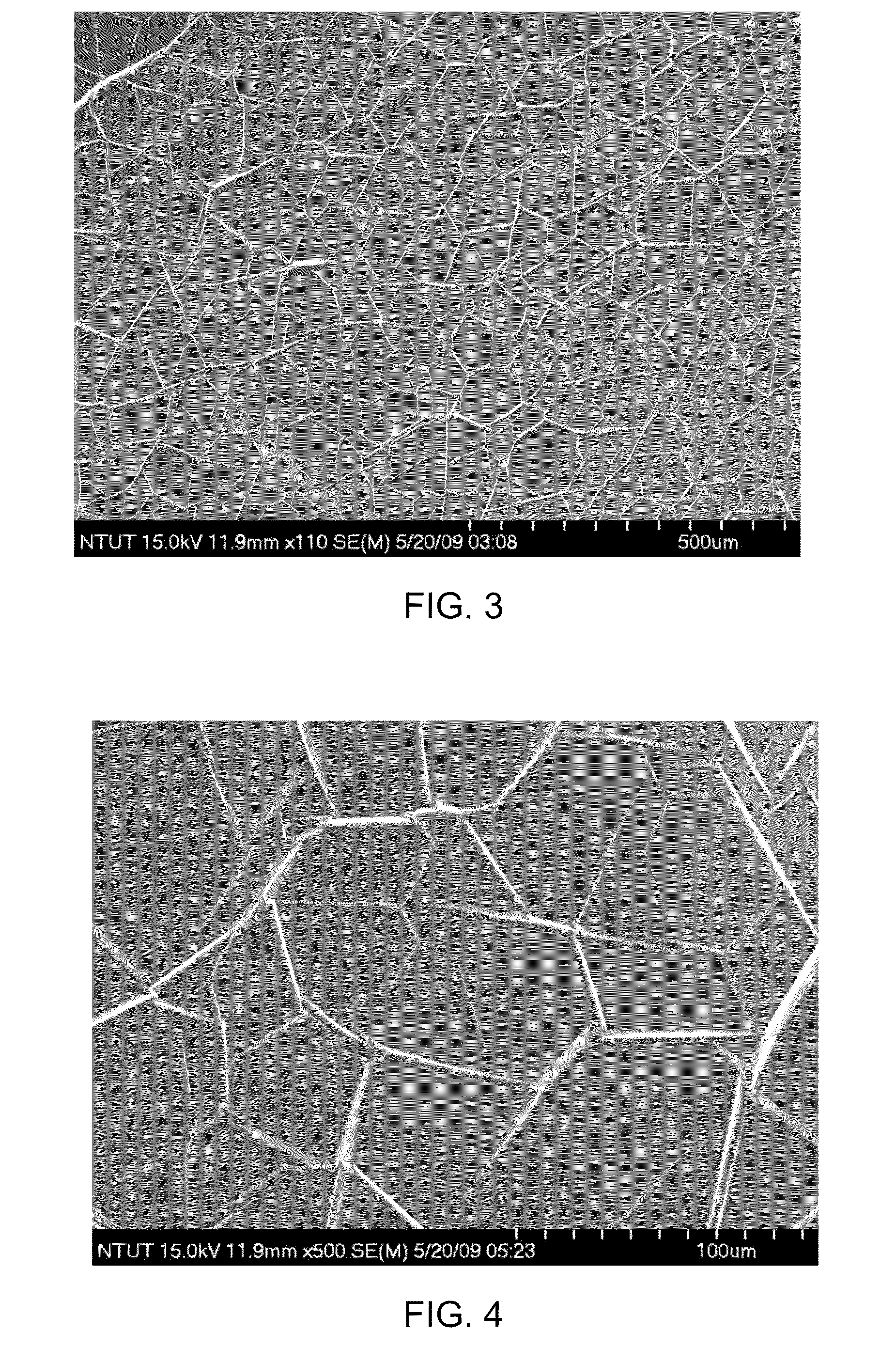
[0072]A graphite block is machined to form a disk-shaped depression with a depth of about 3 mm. A pure nickel plate having a thickness of about 1 mm is placed in the depression. Ultra pure graphite is spread over the nickel plate, and the assembly is placed in a tube furnace. A vacuum is applied to the tube furnace to about 10−5 Torr. The nickel is then fully melted at 1500° C. The nickel maintained in the melted state for 30 to 60 minutes. The temperature is controlled such that the graphite side is about 50° C. hotter than the bath of the molten nickel. Such a temperature disparity reduces convection of the liquid that may disturb the formation of the forming graphene lattice. The furnace is then slowly cooled and the resulting graphene layer is then peeled from the cooled nickel plate.
example 2
[0073]A graphene layer is formed as in Example 1, with the exception that the nickel plated is electrolessly plated with a Ni—P layer. The eutectic point for a Ni—Ni3P layer is 870° C., thus allowing the graphene planes to be formed at 1000° C.
example 3
[0074]A graphene layer is formed as in Example 1, with the exception that the ultra pure graphite is replaced with a blend of ultra pure graphite flakes and carbonyl nickel at 70 wt %.
PUM
| Property | Measurement | Unit |
|---|---|---|
| reactivity | aaaaa | aaaaa |
| size | aaaaa | aaaaa |
| shape | aaaaa | aaaaa |
Abstract
Description
Claims
Application Information