Control of power semiconductor devices

a technology of power semiconductors and semiconductor devices, applied in oscillator generators, pulse techniques, instruments, etc., can solve problems such as current gradients, and achieve the effects of reliable control, optimisation of the performance of both devices, and regulation of current rise rates

Inactive Publication Date: 2010-03-11
MASCHFAB REINHAUSEN GEBR SCHEUBECK GMBH & CO KG
View PDF9 Cites 34 Cited by
  • Summary
  • Abstract
  • Description
  • Claims
  • Application Information

AI Technical Summary

Benefits of technology

[0017]In embodiments the control signal generating circuit comprises at least one digital control loop. For example a rate of change of current may be sensed and used to generate a (1 bit) timing control signal when the di / dt changes from positive to negative (or vice versa). This may be used to identify, approximately, a corner in the diode voltage, identifying a point at which the diode commences to switch. The control signal generating circuit may then generate a control signal to change the voltage on the active switch, for example the collector or emitter voltage of an IGBT, to bring this voltage down rapidly. In embodiments this may be performed by using digital circuitry to control a digital-to-analogue converter in response to the timing control signal. This function may be performed, for example, by high speed digital circuitry and implemented in an FPGA (field programmable gate array). Often switching times are of order nanoseconds and such an arrangement facilitates control on this timescale. Such arrangements facilitate control of the switching active and passive devices in synchronism.
[0021]By means of synchronising the start of the voltage appearing across the freewheel diode with the main voltage fall of the power semiconductor switching device during the switch-on process, the method is able to avoid the reverse recovery voltage overshoot of the freewheel diode and the high current spike of the power semiconductor switching device. It can therefore achieve a safe and efficient current and voltage commutation between the power semiconductor switching device and the freewheel diode with optimised switching losses and switching stresses below desired limits
[0023]In addition, the method is able to permit the regulation of the current rise rate of the power semiconductor switching device during its switch-on operation by circumscribing the voltage fall across the switching device in most conventional circuits which include stray inductance.
[0024]Consequently, the method achieves a reliable control of the inherently non-linear transient behaviours of a power semiconductor switching devices and a freewheel diode, and optimises the performance of both devices in their SOAs (safe operating areas).
[0025]Because of the controlled switching of both the power semiconductor switching device and the freewheel diode, embodiments of the present invention are also a good solution to serial device operation for high power applications, wherein series connection of power semiconductor switching devices such as IGBTs offers an alternative to high voltage thyristors. While IGBTs connected in series are each controlled in accordance with the present method, the switch-on behaviour of individual switch device can be synchronised and the interaction with diodes can be under control. Hence, traditional bulky and expensive switch-on snubber circuit for series connection can be avoided.
[0028]Preferably said instant for the circuit is determined by the change of the diode voltage, but it may instead be generated according to other variables. A simple self-timing method to create the two distinctive stages in said control signal is proposed in the following embodiment. In this the switching device current is monitored and the second stage of the switch-on is delayed until the current in the switching device changes the polarity of its rise rate. In embodiments this approach has the advantage of using feedback loops, making control circuit self-contained and compact.

Problems solved by technology

In embodiments parasitic or other inductance in the circuit, more particularly in the series connected switching device and diode, results in a gradual change of current.

Method used


Image

  • Control of power semiconductor devices
  • Control of power semiconductor devices
  • Control of power semiconductor devices

Examples


Embodiment Construction

[0036]Practical details will now be described with reference to the accompanying drawings.

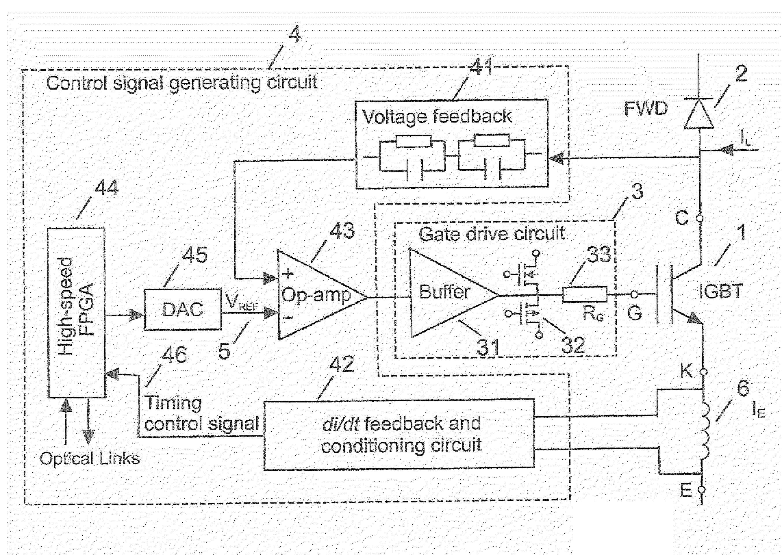
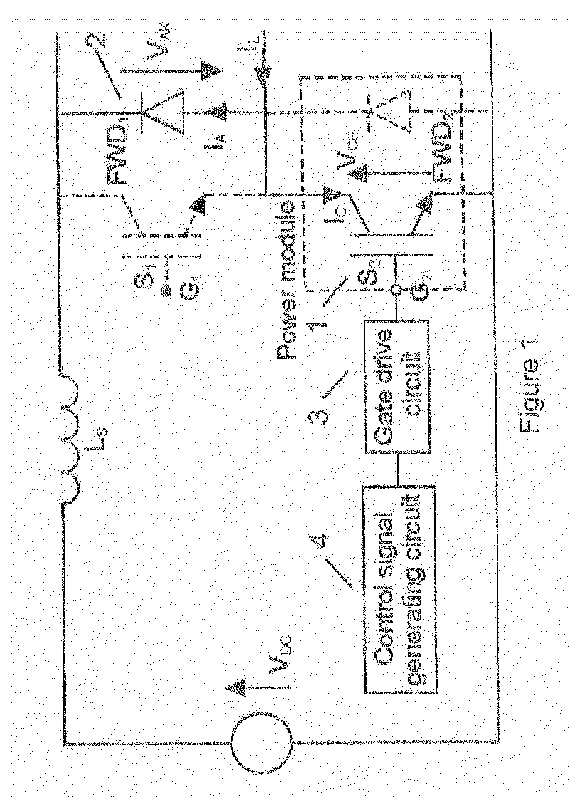
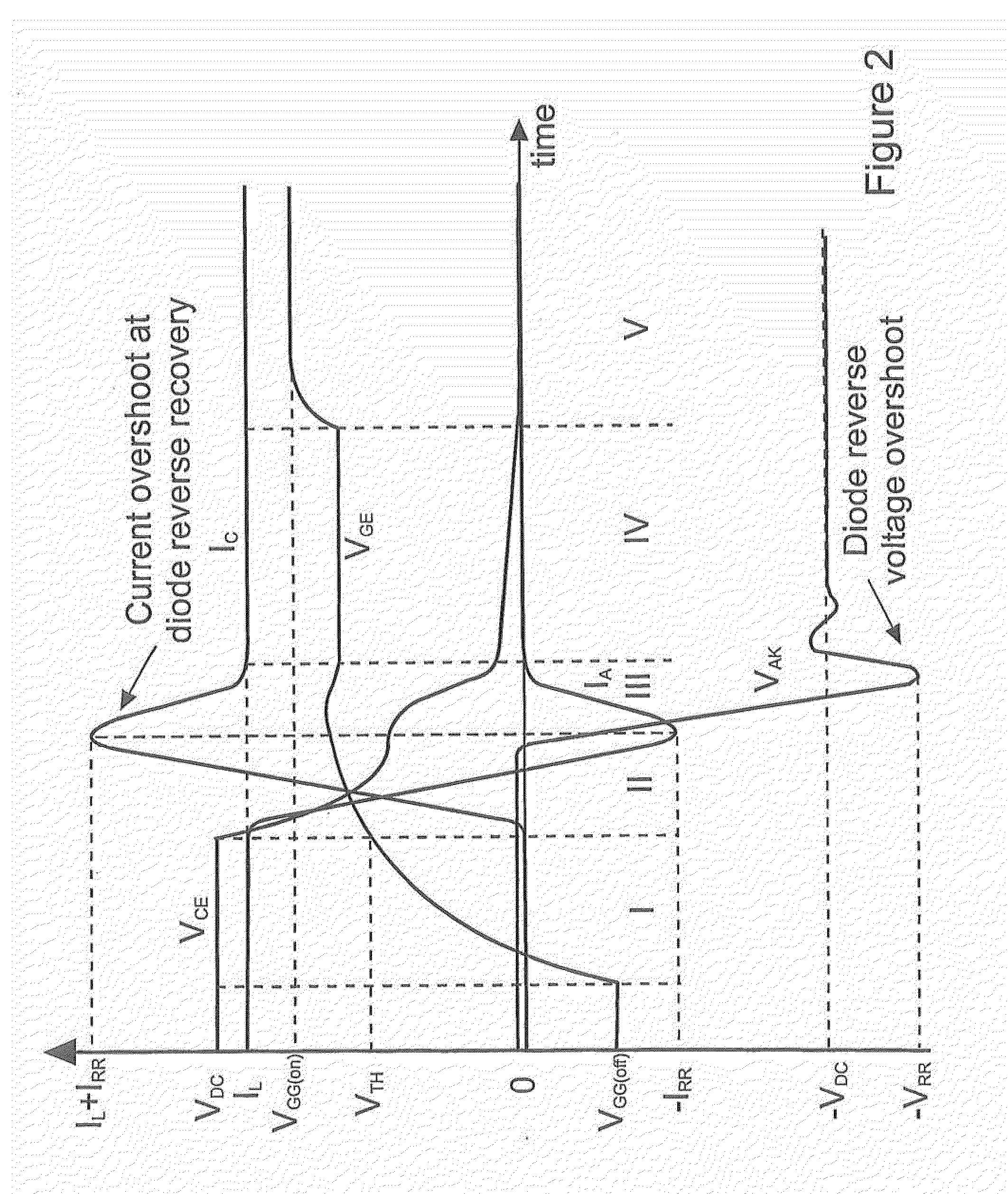
[0037]FIG. 1 shows the circuitry of an embodiment of the present invention applied in a half-bridge circuit, wherein two pairs of power semiconductor switching devices (S1, S2) and freewheel diodes (FWD1, FWD2) are connected as shown in the figure. The half-bridge configuration is the basic topology upon which most inverters are based. As shown in FIG. 1, a freewheel diode is placed in anti-parallel with each power semiconductor switching device. This arrangement normally constitutes a power module. When the upper switching device S1 is on, the lower device S2 is off, and vice-versa. The diodes FWD1 and FWD2 are to provide a path for the inductive load current IL. The current interaction between S2 1 and FWD1 2 is also shown. When the load current IL is flowing in the direction as specified in FIG. 1, the current is commutated from FWD1 2 to S2 1 during a switch-on operation of S2 1. A gate dri...


PUM


Abstract

This invention relates to a control method and a circuit for MOS-gated power semiconductor switching devices such as IGBTs or MOSFETs, which allows control and optimisition of the current and voltage commutation of a power semiconductor switching device and freewheel diode pair in the basic half-bridge circuit found in a wide range of equipment. The method comprises the stages of: applying, upon receipt of a switch-on command signal, a voltage function to the control terminal or the gate of the power semiconductor switching device that allows a regulated current rise in the device whilst maintaining the voltage across the device falling at a predetermined rate; and at the instant when the voltage across the diode begins to change from the on-state towards the off-state level, applying a voltage function to the control terminal or the gate of the power semiconductor switching device to enable the voltage falling across the power semiconductor switching device to track the voltage falling across the diode in order to ensure a fast and controlled completion of the switching operation without diode reverse voltage overshoot. The gate drive automatically modifies the voltage function according to the working condition thereby accounting for the actual operating conditions.

Description

FIELD OF THE INVENTION[0001]This invention generally relates to the control of power semiconductor devices, and in embodiments particularly relates to the concurrent control of power semiconductor switching devices and freewheel diodes.BACKGROUND TO THE INVENTION[0002]Power semiconductor devices are widely in use for a large range of power applications, from low voltage chips, computers, locomotives, to high voltage transmission lines. In most circuits, freewheel diodes need to be used in relation with the power semiconductor switching devices such as IGBTs (insulated gate bipolar transistors) or MOSFETs (metal oxide semiconductor field effect transistors) for a continuous load current conduction to avoid large voltage damaging the semiconductor devices and the circuit. High power IGBTs are often supplied as a module with diodes that act as freewheel diodes within the module. IGBTs are typically found in parallel with the diodes. Reliable switching operation of both a power semicond...

Claims


Application Information

Patent Timeline
Patent Type & Authority Applications(United States)
IPC IPC(8): H03K17/082
CPCH03K17/08148H03K17/168H03K17/166H03K17/0828
Inventor PALMER, PATRICK REGINALDWANG, YALANBRYANT, ANGUS TOBY
Owner MASCHFAB REINHAUSEN GEBR SCHEUBECK GMBH & CO KG
Why Eureka
Try Eureka