In-situ chamber treatment and deposition process

a deposition process and in-situ chamber technology, applied in the direction of chemical vapor deposition coating, liquid surface applicator, coating, etc., can solve the problems of non-uniformity performance after multiple runs are completed in the same ald processing chamber, may have reached the limit of pvd process size and aspect ratio, lack of stability of deposition rate, etc., to achieve the effect of decreasing non-uniformity and increasing uniformity

Active Publication Date: 2010-03-11
APPLIED MATERIALS INC
View PDF106 Cites 48 Cited by
  • Summary
  • Abstract
  • Description
  • Claims
  • Application Information

AI Technical Summary

Benefits of technology

[0015]The treatment of the interior surfaces of the processing chamber during the pretreatment process helps to increase the uniformity (or decrease the non-uniformity) across the substrate surface of the deposited materials—as opposed to not conducting the pretreatment process. The non-uniformity of the deposited material across the substrate surface may be about 12% or less, preferably, about 10% or less, and more preferably, about 8% or less, for example, about 6% or less.

Problems solved by technology

Formation of tantalum-containing layers, such as tantalum, tantalum nitride, and tantalum silicon nitride, in multi-level integrated circuits poses many challenges to process control, particularly with respect to contact formation.
However, it is believed that PVD processes may have reached a limit at this size and aspect ratio, while ALD processes suffer other problems.
Common problems encountered during ALD processes include the lack of stability for the deposition rate and the non-uniformity performance after multiple runs are completed within the same ALD processing chamber.
The secondary reactions result in a drift of the deposition rate and the non-uniformity performance with increasing number of substrates processed within the ALD chamber.
Also, deposited films on the inner surfaces of the processing chamber may peel to form particulates, which end up contaminating the substrate surface.

Method used


Image

  • In-situ chamber treatment and deposition process
  • In-situ chamber treatment and deposition process
  • In-situ chamber treatment and deposition process

Examples


Embodiment Construction

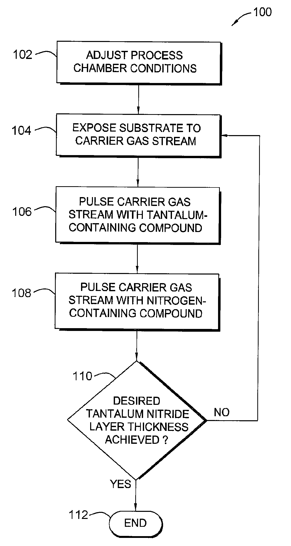
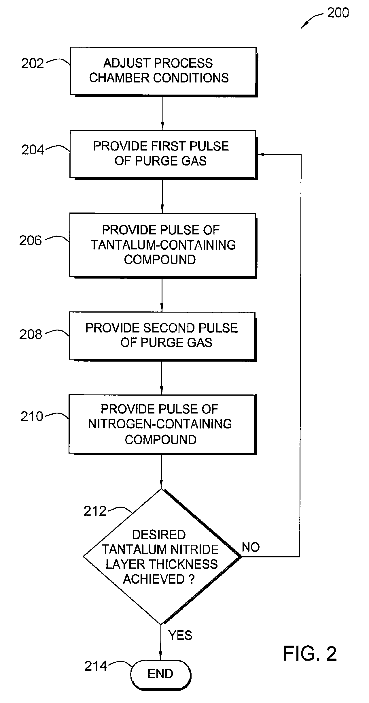
[0021]Embodiments of the invention provide a method for treating the inner surfaces of a processing chamber in situ and depositing a material on a substrate within the processing chamber during a vapor deposition process. The substrate may be sequentially or simultaneously exposed to a first precursor and a second precursor gas during the vapor deposition process, such as atomic layer deposition (ALD) or by chemical vapor deposition (CVD). In one embodiment, the inner surfaces of the processing chamber and the substrate may be exposed to a treatment gas containing a reagent, such as a hydrogenated ligand compound during a pretreatment process. The hydrogenated ligand compound may be the same ligand as a free ligand formed from the metal-organic precursor used during the subsequent vapor deposition process. The free ligand is usually formed by hydrogenation or thermolysis during the deposition process. In one example, the processing chamber and substrate are exposed to an alkylamine ...


PUM

PropertyMeasurementUnit
temperatureaaaaaaaaaa
timeaaaaaaaaaa
temperatureaaaaaaaaaa

Abstract

Embodiments of the invention provide a method for treating the inner surfaces of a processing chamber and depositing a material on a during a vapor deposition process, such as atomic layer deposition (ALD) or by chemical vapor deposition (CVD). In one embodiment, the inner surfaces of the processing chamber and the substrate may be exposed to a reagent, such as a hydrogenated ligand compound during a pretreatment process. The hydrogenated ligand compound may be the same ligand as a free ligand formed from the metal-organic precursor used during the subsequent deposition process. The free ligand is usually formed by hydrogenation or thermolysis during the deposition process. In one example, the processing chamber and substrate are exposed to an alkylamine compound (e.g., dimethylamine) during the pretreatment process prior to conducting the vapor deposition process which utilizes a metal-organic chemical precursor having alkylamino ligands, such as pentakis(dimethylamino) tantalum (PDMAT).

Description

BACKGROUND OF THE INVENTION[0001]1. Field of the Invention[0002]Embodiments of the invention generally relate to semiconductor and other electronic device processing, and more particularly, to an improved method for treating the surfaces of a processing chamber and a substrate therein prior to a vapor deposition process.[0003]2. Description of the Related Art[0004]The electronic device industry and the semiconductor industry continue to strive for larger production yields while increasing the uniformity of layers deposited on substrates having increasingly larger surface areas. These same factors in combination with new materials also provide higher integration of circuits per unit area on the substrate. The need for greater uniformity, deposition rate, and process control regarding layer characteristics rises as the desire for an increased circuit integration. Formation of tantalum-containing layers, such as tantalum, tantalum nitride, and tantalum silicon nitride, in multi-level i...

Claims


Application Information

Patent Timeline
Patent Type & Authority Applications(United States)
IPC IPC(8): H01L21/314
CPCC23C16/34C23C16/4411C23C16/45508H01L21/76843C23C16/45582H01L21/28562C23C16/45531H01L21/205
Inventor MA, PAUL F.AUBUCHON, JOSEPH F.CHANG, MEIKIM, STEVEN H.WU, DIEN-YEHNAKASHIMA, NORMAN M.JOHNSON, MARKPALAKODETI, ROJA
Owner APPLIED MATERIALS INC
Why Eureka
Try Eureka