Wiring board and method of manufacturing the same

Active Publication Date: 2010-03-18
SHINKO ELECTRIC IND CO LTD
View PDF8 Cites 40 Cited by
  • Summary
  • Abstract
  • Description
  • Claims
  • Application Information

AI Technical Summary

Benefits of technology

[0013]An object of the present invention is to provide a wiring board capable of increasing a tensile strength when an external connection terminal or the like is connected to a pad

Problems solved by technology

However, since the Ni layer is readily oxidized, there occurs an inconvenience when a wiring board including the aforementioned two-layer (Au/Ni) structure pad, particularly, a wiring board of a type called “coreless board,” is fabricated.
As a result, when the via is connected to the Ni layer including the oxide formed thereon, an adhesion between the pad and the via decreases due to influence of the oxide, and electrical connection reliability between the pad and the via is damaged.
Then, a problem that the pads are peeled off depending on circumstances possibly arises.
This problem leads to deterioration in performance of the wiring board, and con

Method used


Image

  • Wiring board and method of manufacturing the same
  • Wiring board and method of manufacturing the same
  • Wiring board and method of manufacturing the same

Examples


first embodiment

FIGS. 1 to 4b

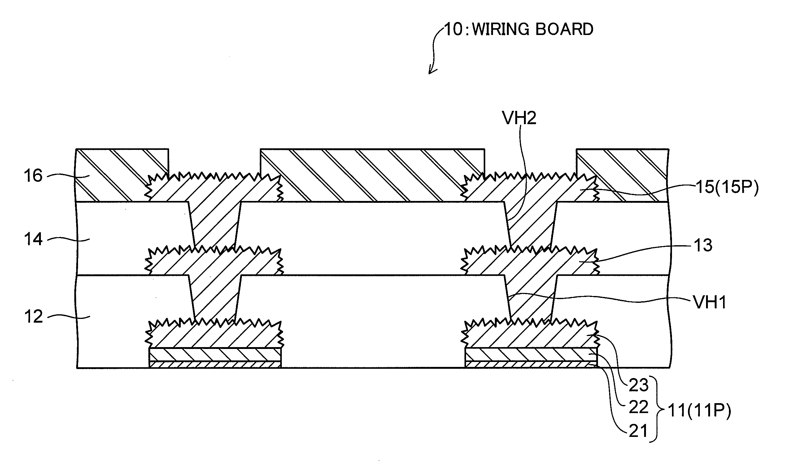
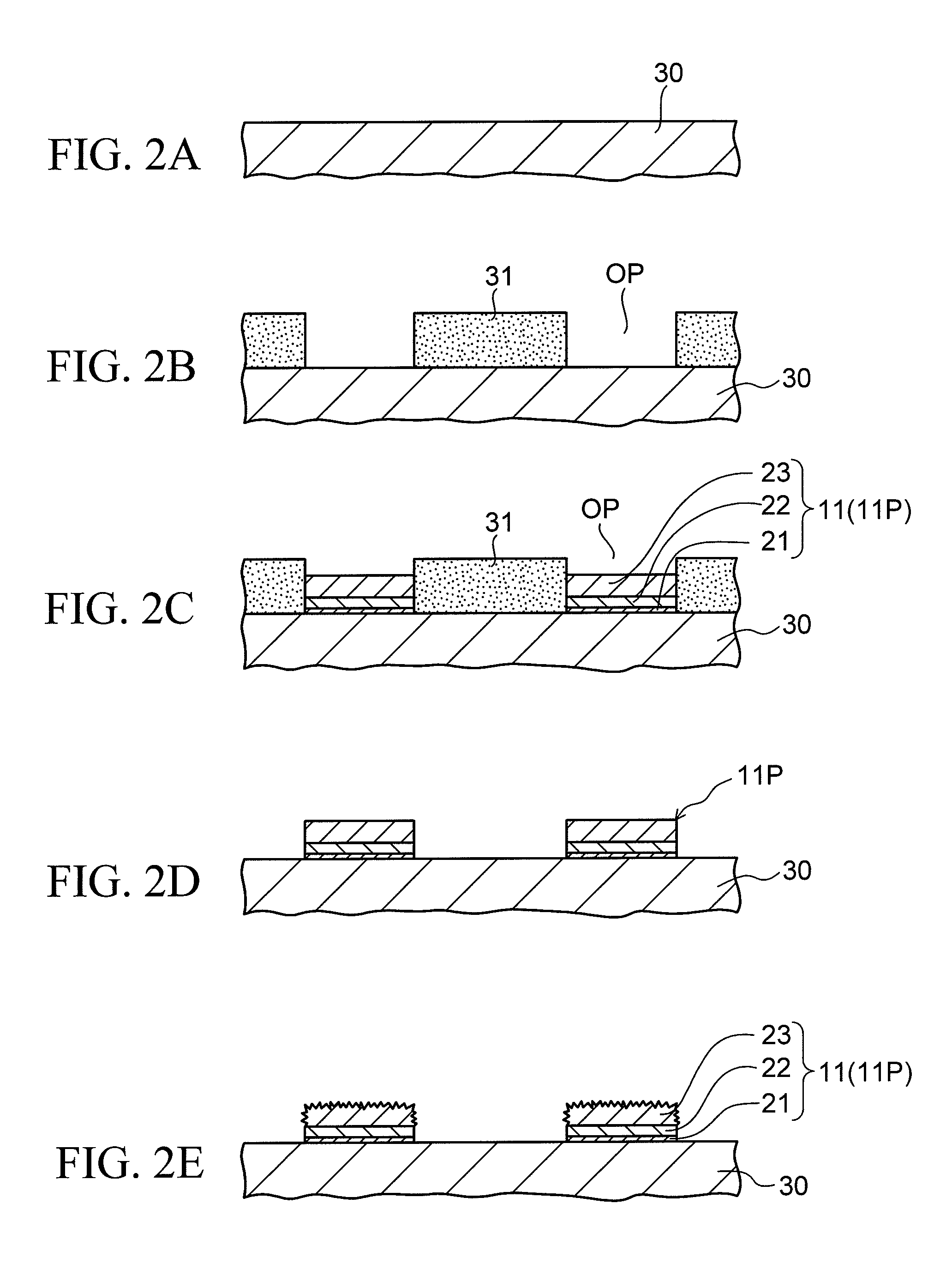
[0030]FIG. 1 is a cross-sectional view showing a configuration of a wiring board (semiconductor package) according to a first embodiment of the present invention.

[0031]As illustrated, a wiring board 10 according to this embodiment has a structure in which multiple wiring layers 11, 13 and 15 are stacked one on top of another with insulating layers (specifically, resin layers) 12 and 14 interposed therebetween. In this structure, the wiring layers 11, 13 and 15 are interlayer connected via conductors (each being a portion of a material forming a corresponding one of the wiring layers 13 and 15) filled into via holes VH1 and VH2 formed on the insulating layers 12 and 14, respectively. Specifically, the wiring board 10 has the form of a “coreless board,” which does not include a support base member and is different from a wiring board fabricated by using a general build-up process (in which a required number of build up layers are sequentially stacked on both surfaces or ...

second embodiment

FIGS. 5 to 7d

[0068]FIG. 5 is a diagram showing a configuration of a wiring board (semiconductor package) according to a second embodiment of the present invention in a form of a cross sectional view.

[0069]As compared with the configuration of the wiring board 10 (FIG. 1) according to the first embodiment, a wiring board 40 according to this embodiment is different in the following points. First, the lower surface of each of pads 41P, which is exposed from the lower side of the insulating layer (resin layer) 12, is formed to be at a position recessed toward an inner side of the board from the lower surface of the insulating layer (resin layer) 12. In addition, each pad 41P is formed of a two-layer structure in which a film (OSP film 51) of water-soluble pre-flux formed on the basis of an OSP (Organic Solderbility Preservative) process, and a metal layer 52 are stacked in layers. In this configuration, the OSP film 51 corresponds to the Au / Pd layer 21 of the pads 11P according to the...

third embodiment

FIGS. 8 to 9c

[0079]FIG. 8 shows a configuration of a wiring board (semiconductor package) according a third embodiment of the present invention in a form of a cross-sectional view.

[0080]As compared with the configuration of the wiring board 10 (FIG. 1) according to the first embodiment, a wiring board 60 according to this embodiment is different in a point that the bottom surface of each of the pads 11P (the bottom surface of the metal layer 21) which is exposed from the lower side of an insulating layer (resin layer) 12a is formed to be at a position recessed from the bottom surface of the insulating layer (resin layer) 12a toward an inside of the board (specifically, the concave portions DP are formed at these portions of the resin layer 12a, and the metal layer 21 of the pads 11P is exposed at these concave portions DP). Since the other configuration thereof is the same as that of the wiring board 10 of the first embodiment, the description thereof is omitted herein.

[0081]The wi...


PUM

PropertyMeasurementUnit
Thicknessaaaaaaaaaa

Abstract

A wiring board includes a pad exposed from an opening portion of an outermost insulating layer. The pad includes: a first metal layer a surface of which is exposed from the wiring board; a second metal layer provided on the first metal layer and formed of a material effective in preventing a metal contained in a via inside the board from diffusing into the first metal layer; and a third metal layer provided between the second metal layer and the via, and formed of a material harder to be oxidized than that of the second metal layer. The thickness of the third metal layer is relatively thick, and is preferably selected to be three times or greater than a thickness of the second metal layer. A side surface of the third metal layer and a surface of the third metal layer to which the via is to be connected are roughed.

Description

CROSS-REFERENCE TO RELATED APPLICATIONS[0001]This application is based on and claims priority of Japanese Patent Application No. 2008-234621 filed on Sep. 12, 2008, the entire contents of which are incorporated herein by reference.BACKGROUND OF THE INVENTION[0002](a) Field of the Invention The present invention relates to a wiring board and a manufacturing method of the same. More particularly, the present invention relates to a wiring board including a pad (a portion of a wiring layer) for use in mounting an electronic component such as a semiconductor element (chip) or in bonding an external connection terminal thereto, and to a manufacturing method of the same.[0003]The wiring board is hereinafter also referred to as a “semiconductor package” for the sake of convenience, in the meaning that the wiring board has the role as a package for mounting a semiconductor element (chip) or the like thereon.[0004](b) Description of the Related Art[0005]In a wiring board, a pad is defined at ...

Claims


Application Information

Patent Timeline
IPC IPC(8): H05K1/02B32B38/00
CPCH01L21/563Y10T156/10H01L23/49816H01L23/49822H01L24/16H01L2224/13099H01L2224/16H01L2224/73203H01L2924/01011H01L2924/01029H01L2924/01046H01L2924/01078H01L2924/01079H01L2924/01082H01L2924/01088H01L2924/15311H05K1/113H05K3/205H05K3/244H05K3/282H05K3/383H05K3/4682H05K2201/09472H05K2201/09563H05K2203/0361H01L2924/01005H01L2924/01006H01L2924/01033H01L2924/01047H05K1/0313H05K1/09H05K3/188H01L2224/16225H01L2224/32225H01L2224/73204H01L21/568Y10T29/4916H01L2224/16235H01L2924/00H01L2924/12042H01L2224/81385H01L2924/00014H01L2924/00011H01L2224/0401
Inventor OGAWA, MICHIROKOBAYASHI, KAZUHIROKANEKO, KENTARO
Owner SHINKO ELECTRIC IND CO LTD
Why Eureka
Try Eureka