Memory device and manufacturing method thereof

a memory device and manufacturing method technology, applied in the field of memory devices, can solve the problems of difficult to achieve high integration, and device structure, and achieve the effects of effective control of charge trap distribution, increased number of times of operation, and prevention of deterioration of memory devices

Inactive Publication Date: 2010-03-18
ELECTRONICS & TELECOMM RES INST
View PDF10 Cites 61 Cited by
  • Summary
  • Abstract
  • Description
  • Claims
  • Application Information

AI Technical Summary

Benefits of technology

[0021]The present invention can provide a resistance variable non-volatile memory device using a trap-controlled SCLC by being provided with a dielectric thin film having a plurality of layers with different charge trap densities.
[0022]In addition, the present invention can effectively control the charge trap distribution in a dielectric thin film by employing an inter-electrode dielectric thin film diffusion prevention film and an internal diffusion prevention film.
[0023]Further, the present invention can prevent migration of charge traps in a dielectric thin film to thus prevent the characteristic of a memory device from being deteriorated with the passage of time and an increase in the number of times of operation by having an internal diffusion prevention film.
[0024]Moreover, the memory device of the present invention has a simple structure, and thus is easily highly integrated and can enhance productivity.

Problems solved by technology

However, since such a flash memory has a structure in which electrons are controlled by applying a high electric field to a floating gate, the device structure becomes relatively complicated as compared to those of other memory devices, thus making it difficult to achieve high integration.
This again makes it difficult to obtain high integration.
However, the ReRAM has the drawback that a high electric driving force is required due to a large amount of current consumed upon operating the device because it shows a metal current characteristic in a low resistance state.
Further, it is not easy to manufacture the ReRAM because the reproducibility of the device is low.

Method used


Image

  • Memory device and manufacturing method thereof
  • Memory device and manufacturing method thereof
  • Memory device and manufacturing method thereof

Examples


first embodiment

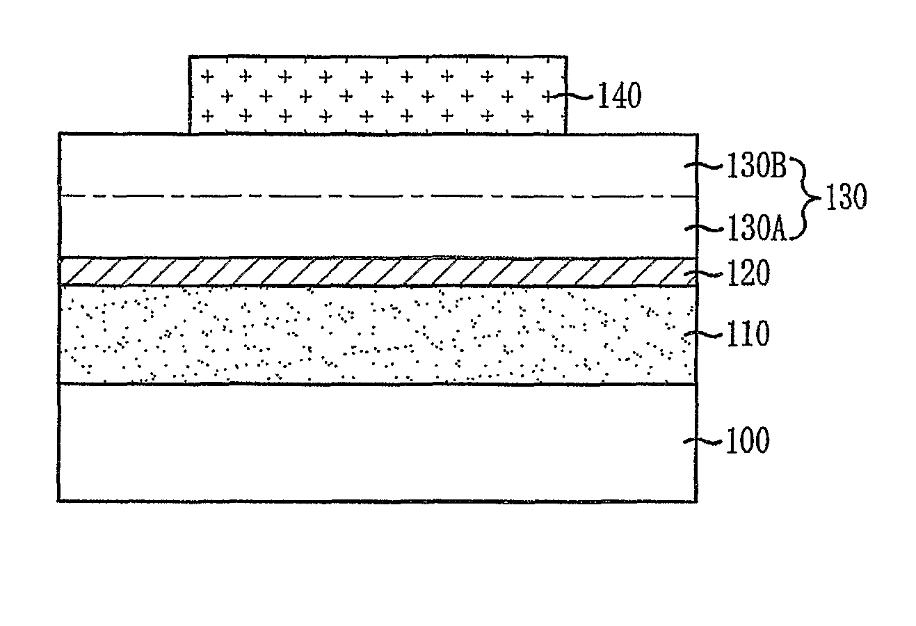
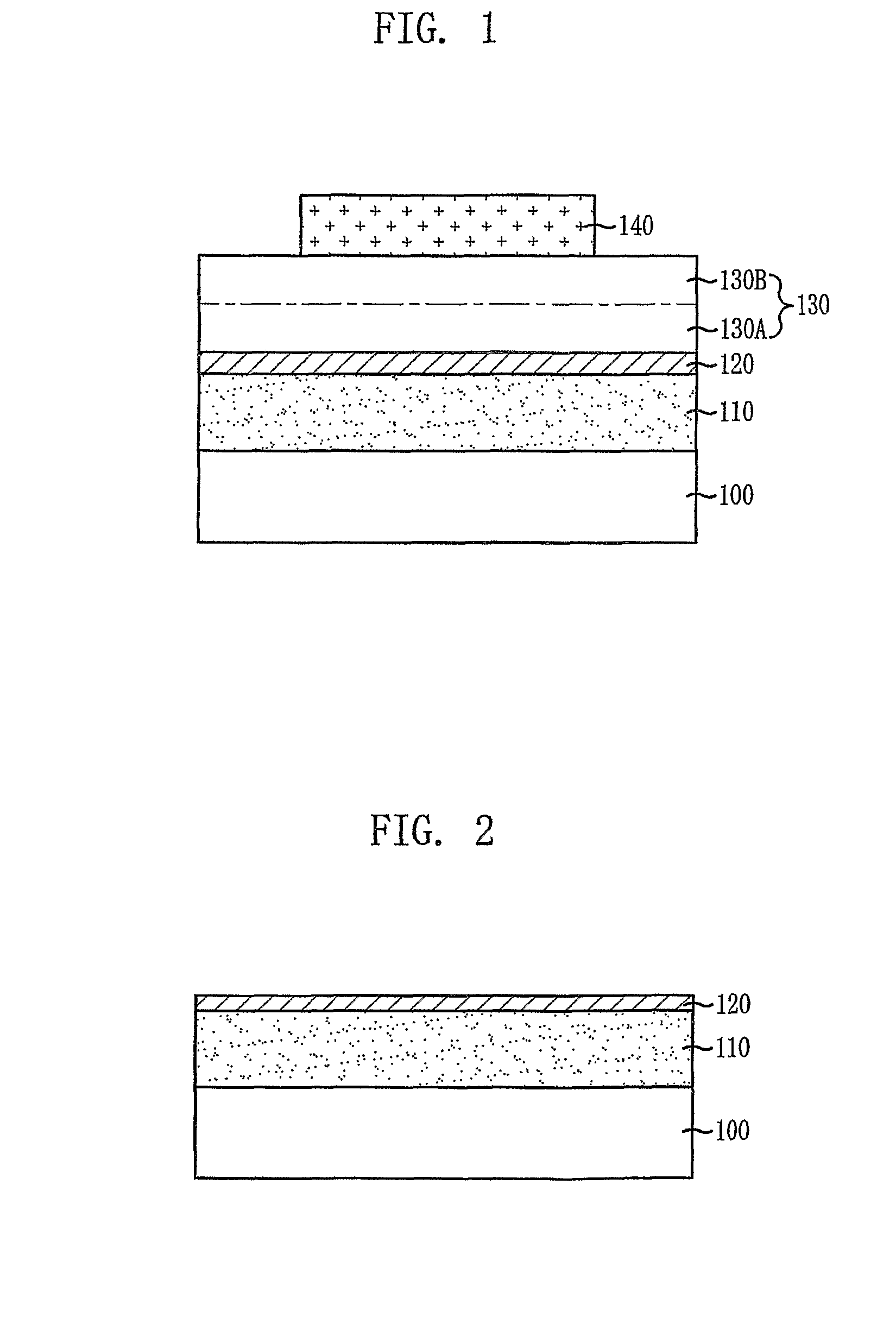
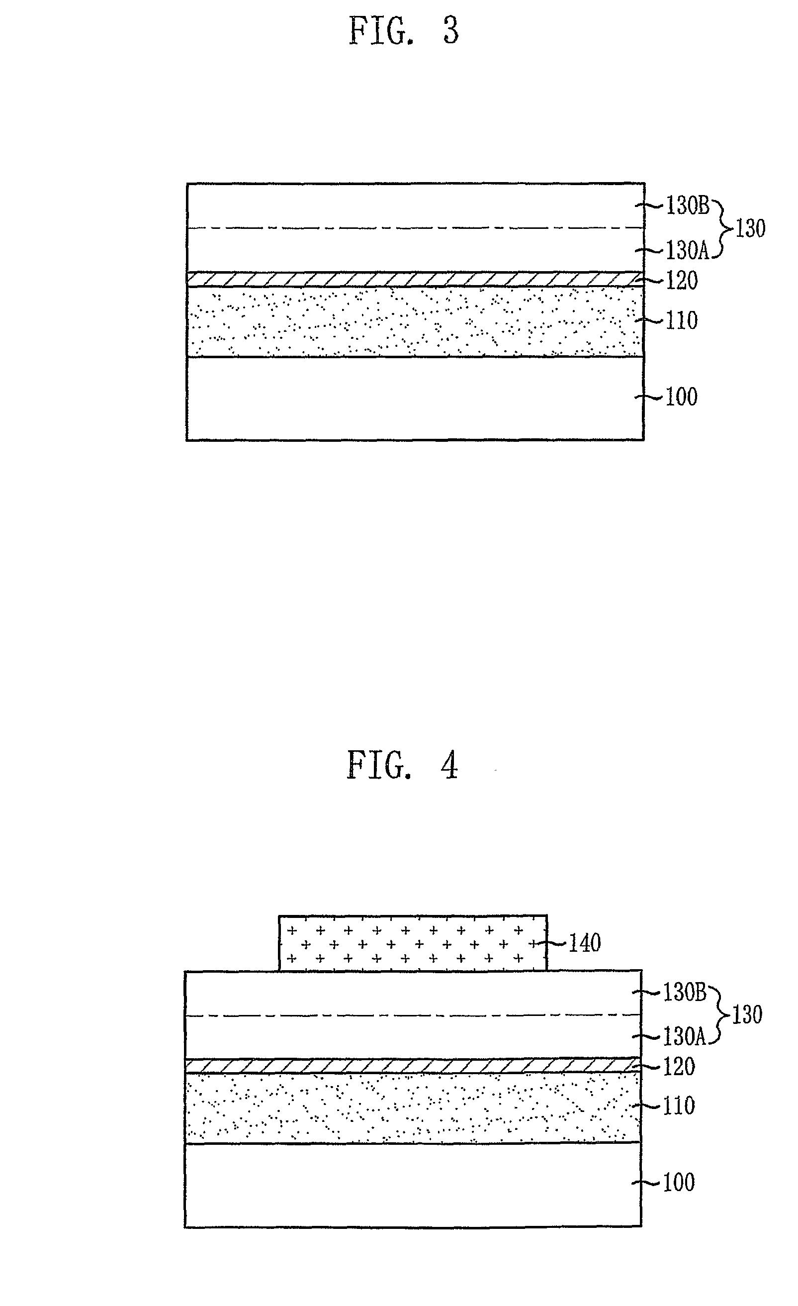
[0059]FIG. 1 is a cross-sectional view of a memory device in accordance with the present invention.

[0060]As shown in FIG. 1, the memory device in accordance with the first embodiment of the present invention includes a substrate 100, a bottom electrode 110 formed on the substrate 100, an inter-electrode dielectric thin film diffusion prevention film 120 formed on the bottom electrode 110, a dielectric thin film 130 formed on the interelectrode dielectric thin film diffusion prevention film 120 and having a structure having a plurality of layers 130A and 130B with different charge trap densities, and a top electrode 140 formed on the dielectric thin film 130. The plurality of layers 130A and 130B in the dielectric thin film 130 may be formed of the same dielectric material or a different dielectric material. In the first embodiment of the present invention, the same dielectric material is used.

[0061]The dielectric thin film 130 is formed to have a relatively thin thickness so as to f...

second embodiment

[0082]FIG. 5 is a cross-sectional view showing a memory device in accordance with the present invention.

[0083]As shown in FIG. 5, the memory device in accordance with the second embodiment of the present invention includes a substrate 200, a bottom electrode 210 formed on the substrate 200, an inter-electrode dielectric thin film diffusion prevention film 220 formed on the bottom electrode 210, a dielectric thin film 230 formed on the interelectrode dielectric thin film diffusion prevention film 220 and having a structure having a plurality of layers 230A and 230B with different charge trap densities, an internal diffusion prevention film 250 for preventing migration of charge traps between the layers in the dielectric thin film, and a top electrode 240 formed on the dielectric thin film 230. The plurality of layers 230A and 230B in the dielectric thin film 230 may be formed of the same dielectric material or a different dielectric material.

[0084]The dielectric thin film 130 is form...


PUM


Abstract

Provided is a resistance variable non-volatile memory device using a trap-controlled Space Charge Limited Current (SCLC), and a manufacturing method thereof. The memory device includes a bottom electrode; an inter-electrode dielectric thin film diffusion prevention film formed on the bottom electrode; a dielectric thin film formed on the inter-electrode dielectric thin film diffusion prevention film and having a plurality of layers with different charge trap densities; and a top electrode formed on the dielectric thin film.

Description

TECHNICAL FIELD[0001]The present invention relates to a memory device and a manufacturing method thereof; and more particularly, to a resistance variable non-volatile memory device using a trap-controlled Space Charge Limited Current (SCLC), and a manufacturing method thereof.BACKGROUND ART[0002]As various types of electronic products, such as portable computers, mobile phones, MP3 players, and digital cameras, gradually get smaller and multifunctional, there is growing demand for low power and high integration of a non-volatile memory device that is an information storage device used for these devices.[0003]Currently, flash memories based on the control of electrons in a floating gate are taking the lead in the non-volatile memory technology. However, since such a flash memory has a structure in which electrons are controlled by applying a high electric field to a floating gate, the device structure becomes relatively complicated as compared to those of other memory devices, thus m...

Claims


Application Information

Patent Timeline
Patent Type & Authority Applications(United States)
IPC IPC(8): H01L45/00H01L21/28
CPCH01L45/10H01L45/12H01L45/1233H01L45/1616H01L45/1625G11C13/0007H01L45/146G11C2013/009G11C2213/15G11C2213/32G11C2213/34G11C2213/51G11C2213/55G11C13/0069H10N70/25H10N70/801H10N70/023H10N70/026H10N70/8833H10N70/826H10N70/882
Inventor CHOI, SUNG-YOOLRYU, MIN-KIJEONG, HU-YOUNG
Owner ELECTRONICS & TELECOMM RES INST
Why Eureka
Try Eureka