Nanotube Device Having Nanotubes with Multiple Characteristics

a technology of nanotubes and nanotubes, applied in the direction of semiconductor devices, electrical devices, molecular computers, etc., can solve the problems of primary source of wasted energy in power semiconductor devices, and achieve the effect of significantly less energy consumption

Inactive Publication Date: 2010-03-18
ETAMOTA CORP
View PDF36 Cites 16 Cited by
  • Summary
  • Abstract
  • Description
  • Claims
  • Application Information

AI Technical Summary

Benefits of technology

[0010]A carbon nanotube of a nanotube device has at least two segments with different characteristics. The segments meet at a junction and a diameter of the carbon nanotube on either side of the junction is about the same. One segment may be doped differently from another segment. One segment may be p doped and another segment n dop

Problems solved by technology

More specifically, a primary source of wasted energy in power semiconductor devi

Method used


Image

  • Nanotube Device Having Nanotubes with Multiple Characteristics
  • Nanotube Device Having Nanotubes with Multiple Characteristics
  • Nanotube Device Having Nanotubes with Multiple Characteristics

Examples


Embodiment Construction

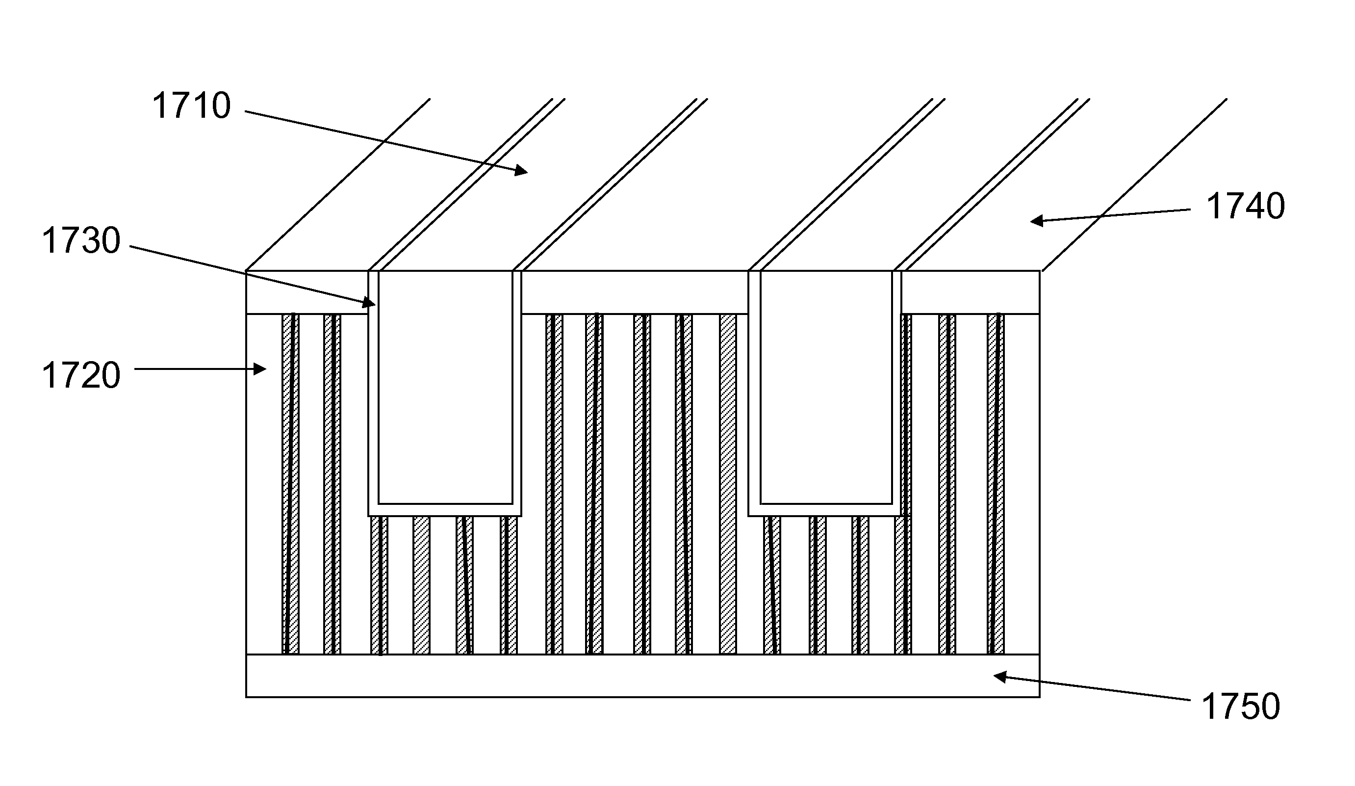
[0044]The invention provides a carbon nanotube device and techniques for manufacturing such a device. The device includes nanotubes having multiple properties or characteristics. The nanotubes may be single-walled or multiwalled carbon nanotubes. For example, a carbon nanotube device may be made of multiple nanotubes, each nanotube having two or more segments, where segments have different properties or characteristics from adjacent segments. For example, one segment may be an n-type semiconductor material and another segment may be a p-type semiconductor material. There is a junction where two segments meet. This carbon nanotube device may be part of a diode or other semiconducting device. The device may be a power or high-power device, capable of passing relatively high currents compared to standard devices.

[0045]In a specific embodiment, the carbon nanotube technology of the invention is incorporated in a carbon nanotube transistor. The carbon nanotube transistor may be a single-...


PUM


Abstract

A carbon nanotube of a nanotube device has at least two segments with different characteristics. The segments meet at a junction and a diameter of the carbon nanotube on either side of the junction is about the same. One segment may be doped differently from another segment. One segment may be p doped and another segment n doped. One segment may be doped with a different carrier concentration from another segment. The nanotube device may be used in power semiconductor devices including power diodes and power transistors. These power devices will be very power efficient, wasting significantly less energy than similar manufactured using silicon technology.

Description

[0001]This application claims the benefit of U.S. provisional patent application 60 / 653,074, filed Feb. 14, 2005 and is a continuation-in-part of U.S. patent application Ser. No. 11 / 162,548, filed Sep. 14, 2005, which are all incorporated by reference along with other references cited in this application.BACKGROUND OF THE INVENTION[0002]The present invention relates to semiconductor devices and their manufacture, and more specifically to carbon nanotube device technology.[0003]The age of information and electronic commerce has been made possible by the development of transistors and electronic circuits, and their miniaturization through integrated circuit technology. Integrated circuits are sometimes referred to as “chips.” Many numbers of semiconductor devices including transistors and diodes are used to build electronic circuits and integrated circuits. Modern microprocessor integrated circuits have over 50 million transistors and will have over 1 billion transistors in the future...

Claims


Application Information

Patent Timeline
IPC IPC(8): H01L29/66H01L21/336
CPCB82Y10/00H01L51/057G06N99/007H10K10/491
Inventor TOMBLER, JR., THOMAS W.
Owner ETAMOTA CORP
Why Eureka
Try Eureka