
Content-Addressable Memory

a content and memory technology, applied in the field of content-addressable memory, can solve the problems of increasing power consumption and overall efficiency, and achieve the effect of high operating speed and low power consumption

Active Publication Date: 2010-03-18
REALTEK SEMICON CORP
View PDF4 Cites 6 Cited by
  • Summary
  • Abstract
  • Description
  • Claims
  • Application Information

AI Technical Summary

Benefits of technology

The invention is about a content-addressable memory (CAM) that has high operating speed and low power consumption. The CAM has two parts: a first memory unit and a second memory unit. The first memory unit has a data memory cell and a comparison circuit for comparing a search bit with the data bit and outputting a match result. The second memory unit has a data memory cell and a comparison circuit for comparing a search bit with the data bit and outputting a match result. The first static CMOS logic circuit performs a logic operation on the match result and the second comparison result to output a final match result. The technical effect of this invention is to provide a faster and more efficient CAM for comparing data bits and performing logic operations.

Problems solved by technology

As a result, overall efficiency is reduced and power consumption is increased.

Method used


Image

  • Content-Addressable Memory
  • Content-Addressable Memory
  • Content-Addressable Memory

Examples


first preferred embodiment

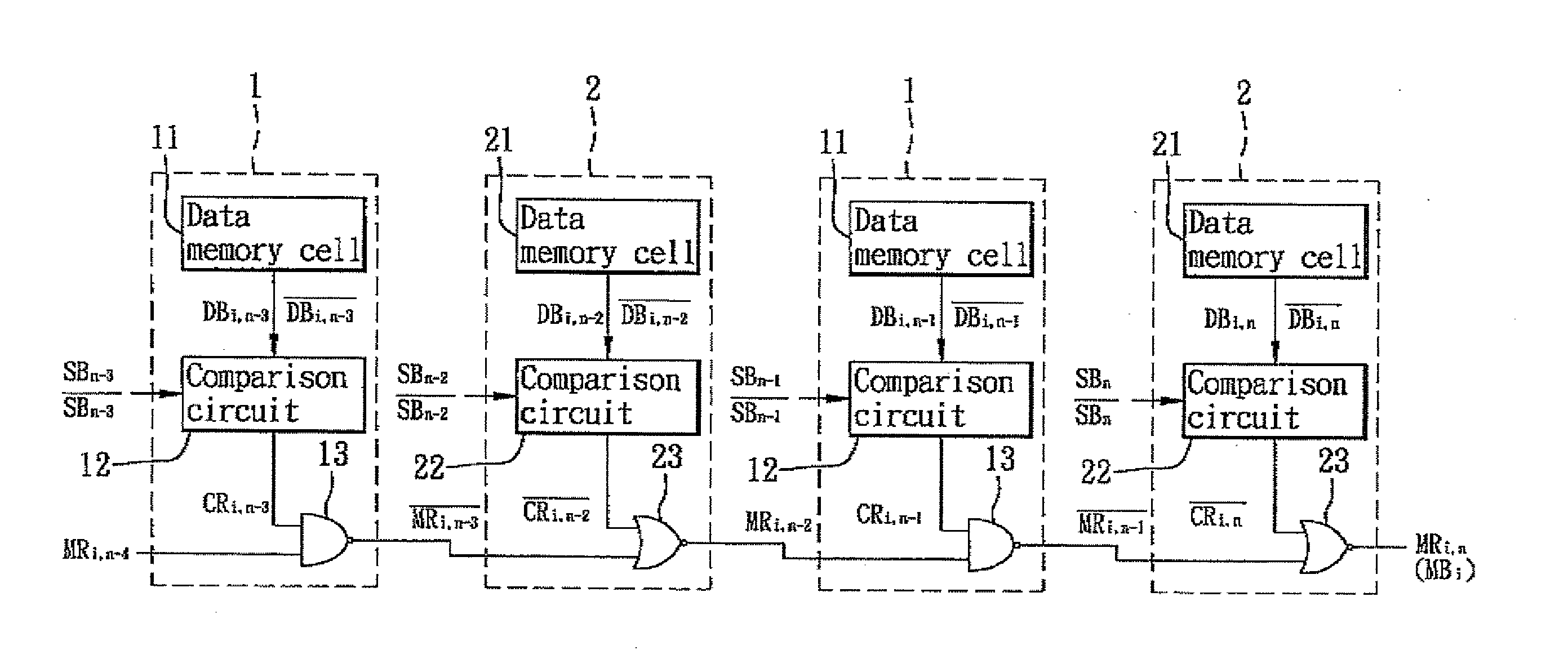
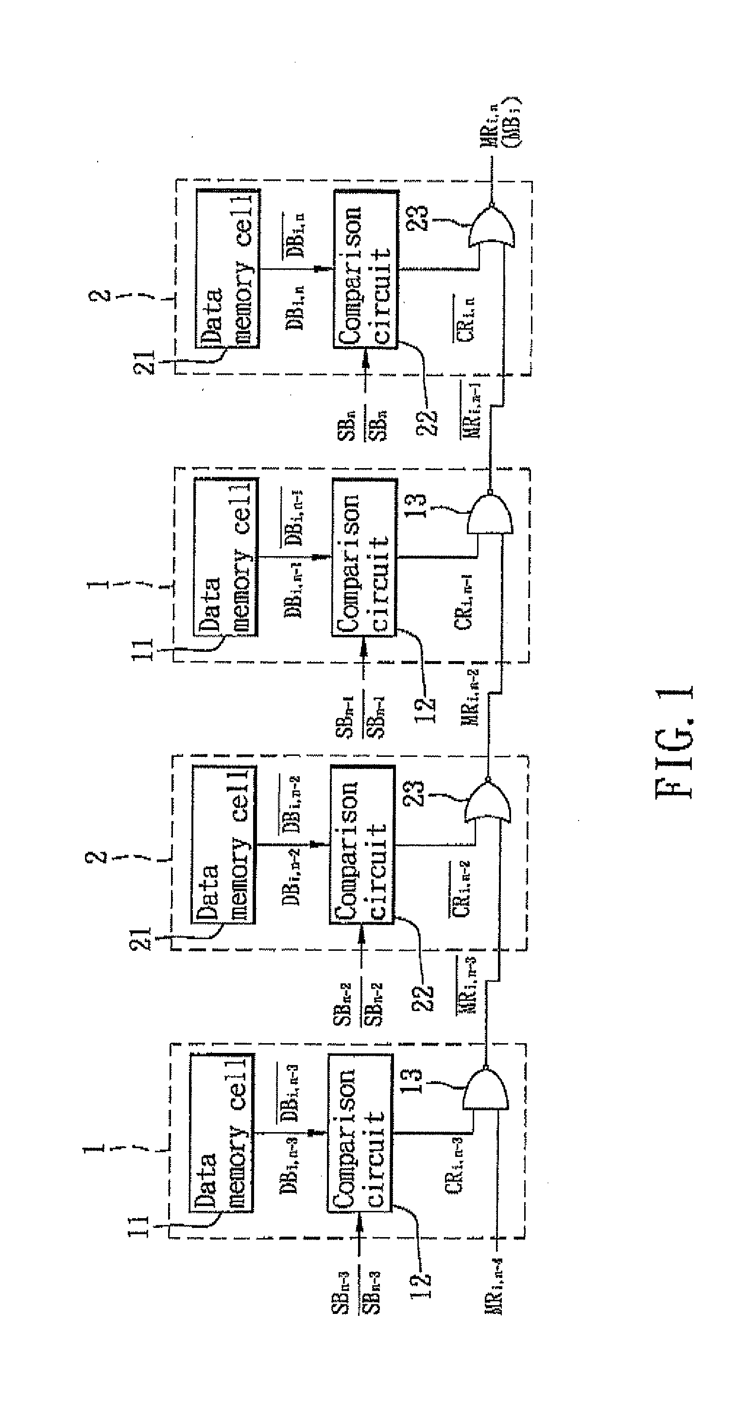
[0026]Referring to FIG. 1, the first preferred embodiment of a CAM according to the present invention is a binary CAM, and includes a plurality of memory units 1 and a plurality of memory units 2 (in FIG. 1, only the last four memory units 1, 2 on an ith row are shown). For each row, the memory units 1 are alternatingly disposed with the memory units 2, and each memory unit 1, 2 receives one of the n-number of search bits SBj and one of the n-number of complementary search bits SBj.

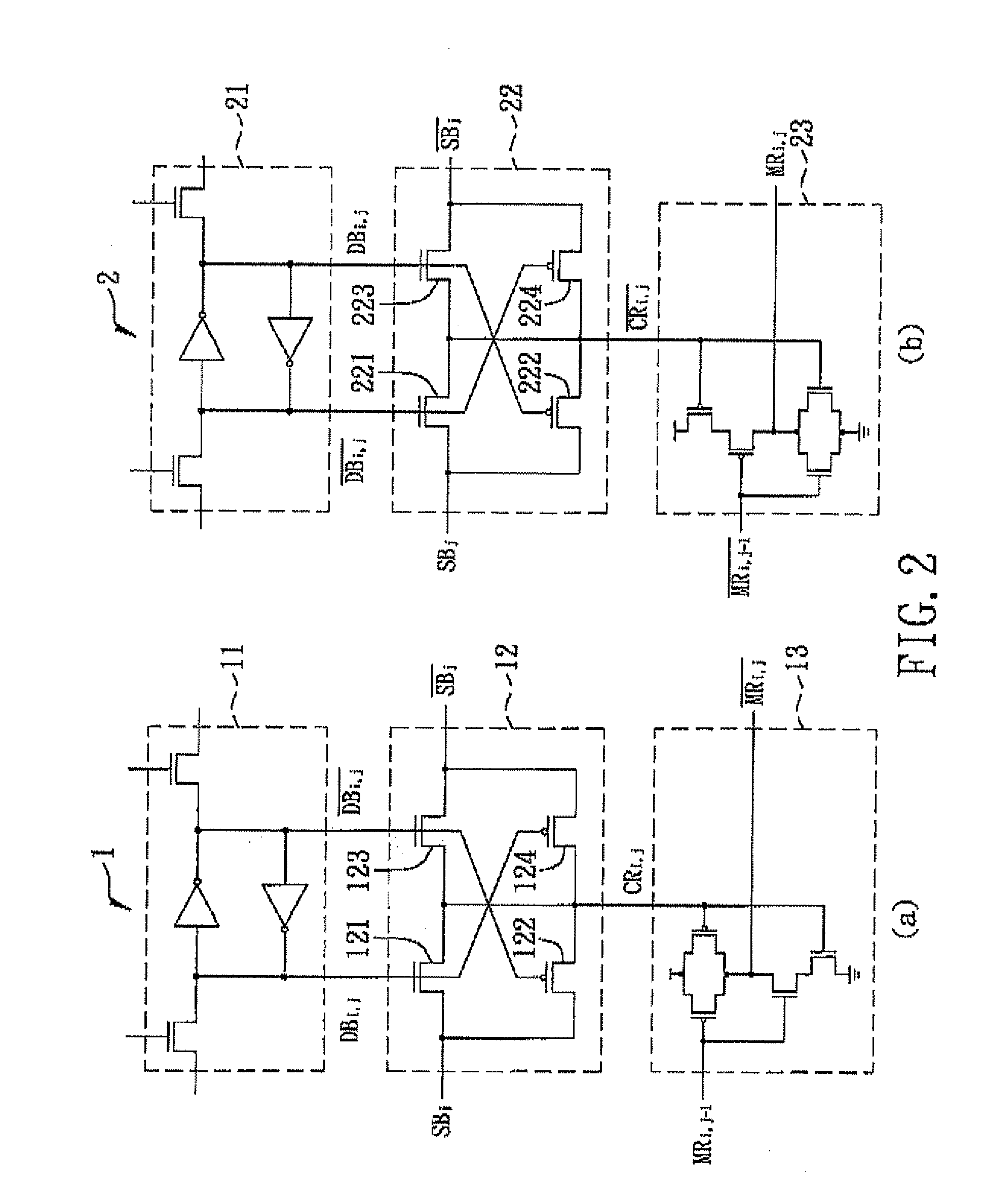
[0027]Each memory unit 1 includes a data memory cell 11, a comparison circuit 12, and a static complementary metal-oxide-semiconductor (CMOS) logic circuit 13. The data memory cell 11 stores a data bit DBi,j and a complementary data bit DBi,j. The comparison circuit 12 is coupled to the data memory cell 11, receives the corresponding search bit SBj, the corresponding complementary search bit SBj, and the data bit DBi,j and complementary data bit DBi,j stored in the data memory cell 11, compares the corres...

second preferred embodiment

[0034]Referring to FIG. 3, the second preferred embodiment of a CAM according to the present invention is a binary CAM, and includes a plurality of memory units 3 and a plurality of memory units 4 (in FIG. 3, only the last two memory units 3, 4 on an ith row are shown). For each row, the memory units 3 are alternatingly disposed with the memory units 4, and each memory unit 3, 4 receives two of the n-number of search bits SBj and two of the n-number of complementary search bits SBj.

[0035]Each memory unit 3 includes two data memory cells 31, 32, two comparison circuits 33, 34, and a static CMOS logic circuit 35. The data memory cell 31 stores a data bit DBi,j and a complementary data bit DBi,j. The data memory cell 32 stores a data bit DBi,j-1 and a complementary data bit DBi,j-1. The comparison circuit 33 is coupled to the data memory cell 31, receives the corresponding search bit SBj, the corresponding complementary search bit SBj, and the data bit DBi,j and complementary data bit ...

third preferred embodiment

[0040]Referring to FIG. 6, the third preferred embodiment of a CAM according to the present invention is a ternary CAM, and includes a plurality of memory units 5 and a plurality of memory units 6 (in FIG. 6, only the last four memory units 5, 6 on an ith row are shown). For each row, the memory units 5 are alternatingly disposed with the memory units 6, and each memory unit 5, 6 receives one of the n-number of search bits SBj, and one of the n-number of complementary search bits SBj.

[0041]Each memory unit 5 includes a data memory cell 51, a mask memory cell 52, a comparison circuit 53, and a static CMOS logic circuit 54. The data memory cell 51 stores a data bit DBi,j. The mask memory cell 52 stores a mask bit CBi,j. The comparison circuit 53 is coupled to the data memory cell 51 and the mask memory cell 52, receives the corresponding search bit SBj, the corresponding complementary search bit SBj, the data bit DBi,j stored in data memory cell 51, and the mask bit CBi,j stored in th...


PUM


Abstract

A CAM includes first and second memory units. The first memory unit includes: a first data memory cell for storing a first data bit; a first comparison circuit for comparing a first search bit with the first data bit to determine if there is a match, and outputting a first comparison result; and a first CMOS logic circuit for performing a logic operation on the first comparison result and outputting a first matching result. The second memory unit includes: a second data memory cell for storing a second data bit; a second comparison circuit for comparing a second search bit with the second data bit to determine if there is a match, and outputting a second comparison result; and a second static CMOS logic circuit for performing a logic operation on the first matching result and the second comparison result, and outputting an output matching result.

Description

CROSS-REFERENCE TO RELATED APPLICATION[0001]This application claims priority to Taiwanese Application No. 097135791, filed on Sep. 18, 2008.1. FIELD OF THE INVENTION[0002]The present invention relates to a content-addressable memory (CAM), more particularly to a CAM that can save the step of precharging.2. DESCRIPTION OF THE RELATED ART[0003]A CAM comprises a plurality of CAM cells arranged in an array. Content stored in each row of the array is compared with search data to determine if there a match, and a plurality of matching bits corresponding respectively to the rows are generated in accordance with the results of such a comparison.[0004]Depending on the number of states that can be stored by the CAM cells, a CAM is classified as a binary CAM or a ternary CAM.[0005]In the case of the binary CAM, each CAM cell includes a data memory cell and a comparison circuit. The data memory cell stores a data bit and a complementary data bit to represent one of either a “0” or “1” state.[00...

Claims


Application Information

Patent Timeline
Patent Type & Authority Applications(United States)
IPC IPC(8): G11C15/04
CPCG11C15/04G11C15/00
Inventor CHIANG, MING-CHENG
Owner REALTEK SEMICON CORP
Learn More