Semiconductor device

Inactive Publication Date: 2010-03-25
HITACHI LTD
View PDF5 Cites 13 Cited by
  • Summary
  • Abstract
  • Description
  • Claims
  • Application Information

AI Technical Summary

Benefits of technology

[0015]With the semiconductor device according to the present invention, hi

Problems solved by technology

With the current-drive type D-A converter, in the case of any of the methods described is adopted, a relative error

Method used


Image

  • Semiconductor device
  • Semiconductor device
  • Semiconductor device

Examples


Example

First Embodiment

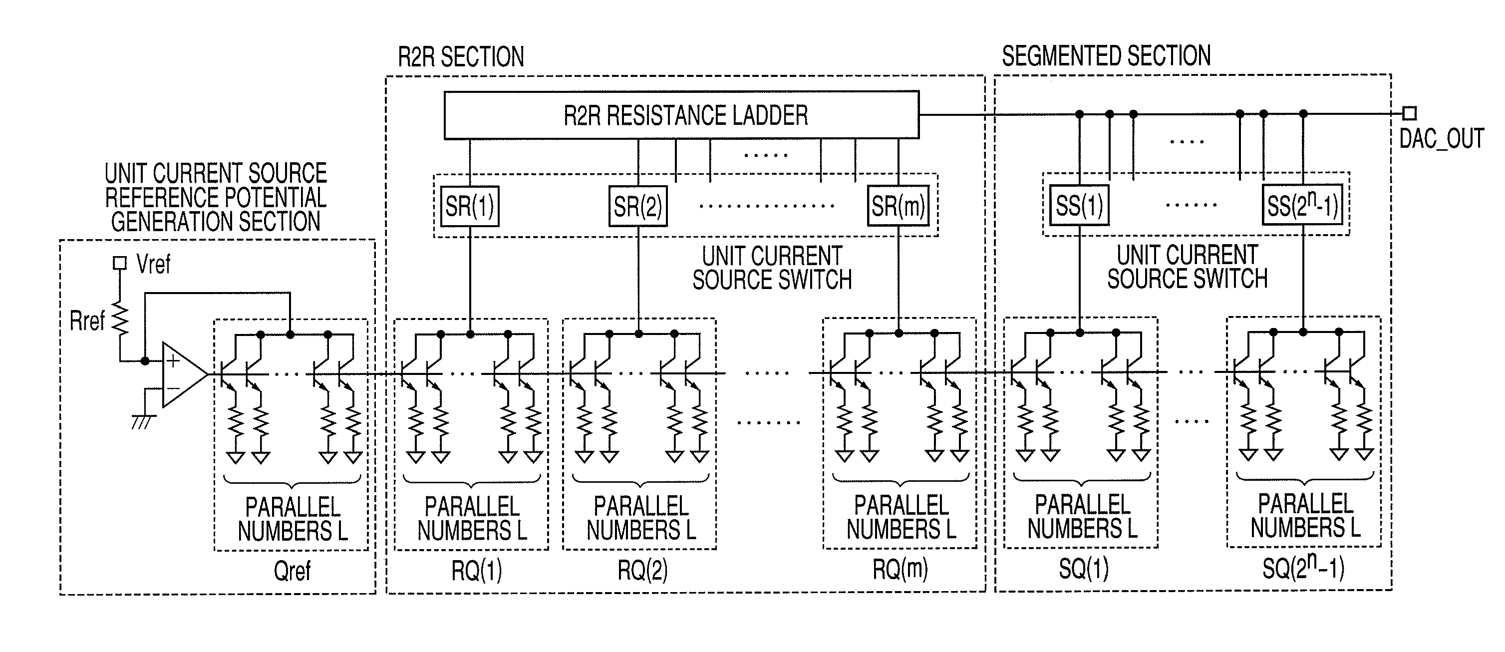
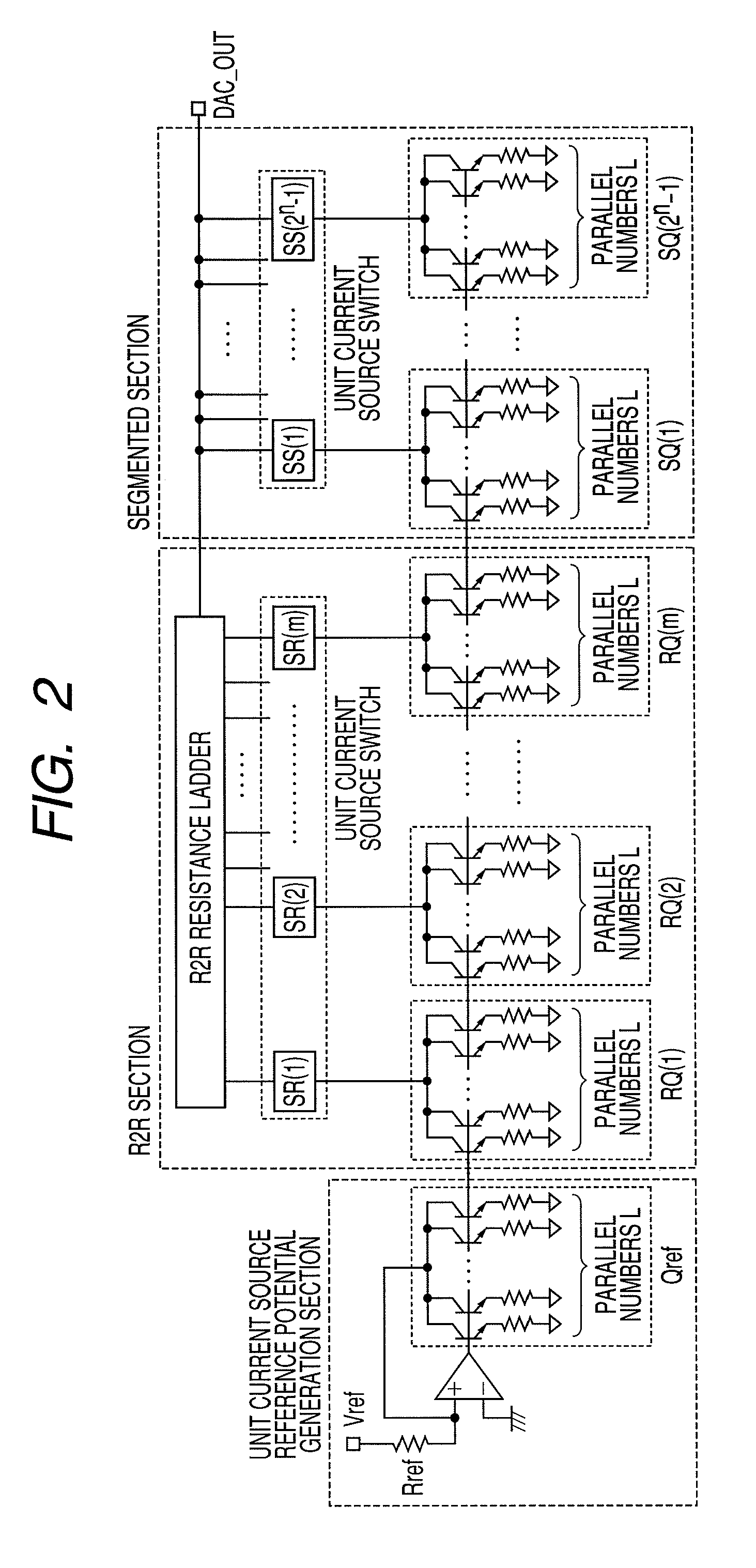
[0027]FIG. 5 is a block diagram showing an example of a configuration of a segmented R2R type D-A converter according to a first embodiment of the invention. In the case of the present D-A converter, with respect to not only unit current sources SQ(1) to SQ(2n−1) of a segmented section thereof, but also unit current sources RQ(1) to RQ(m) of an R2R section thereof, the unit current sources are disposed so as to be evenly spread out distancewise in a current source dispersedly laid-out region, the unit current sources each being composed of plural current source elements arranged in parallel numbers L. Since the respective unit current sources SQ(1) to SQ(2n−1) and RQ(1) to RQ(m) are composed of the plural current source elements undergoing parallel operations (the parallel numbers L), a random relative error attributable to production tolerance is reduced to 1 / √{square root over (L)}, and since the plural current source elements undergoing parallel operations in the ...

Example

Second Embodiment

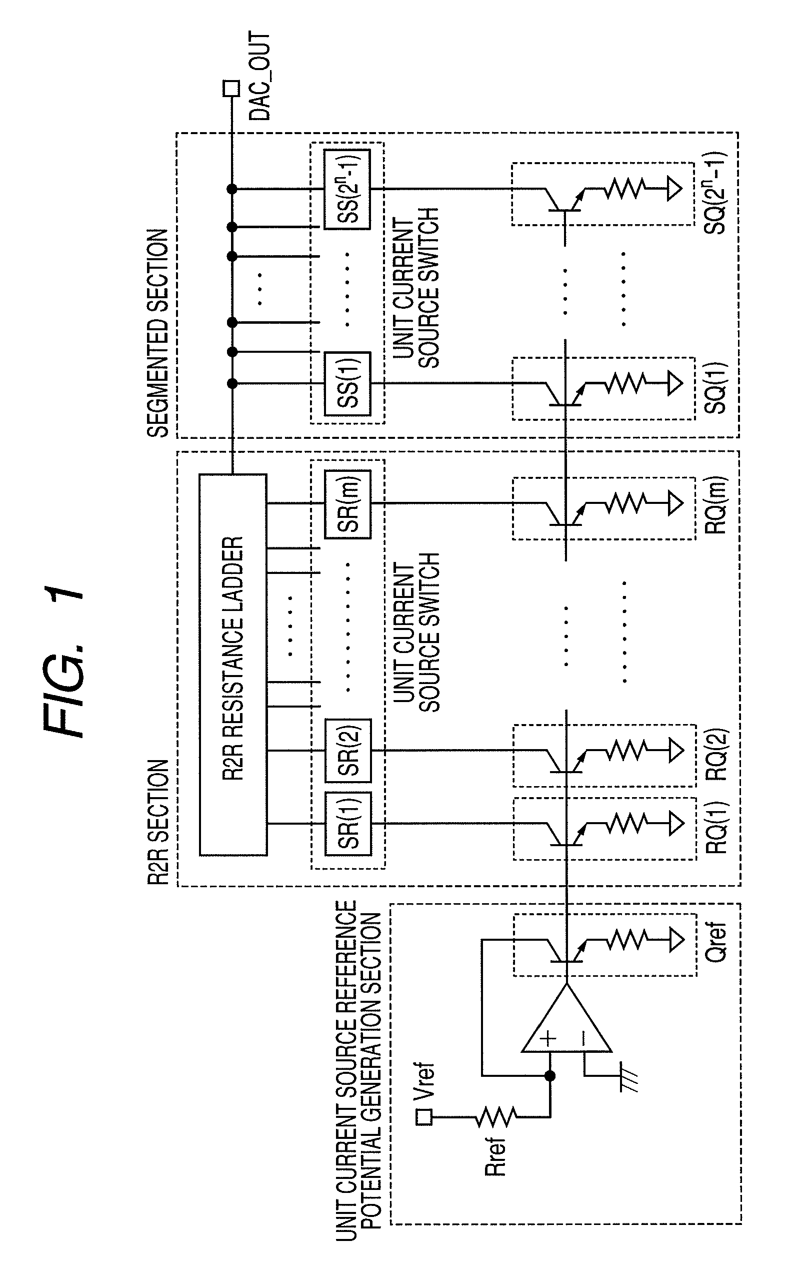
[0029]FIG. 6 is a block diagram showing another example of a configuration of a segmented R2R type D-A converter according to a second embodiment of the invention. As shown in FIG. 6, unit current source switches SS (1) to SS (2n−1) of a segmented section, and unit current source switches SR(1) to SR(m) of an R2R section, disposed in a concentrated manner within a switch concentratedly laid-out region are each connected to the collector of an NPN bipolar transistor with a base potential biased at a given potential, and the emitter of each of the NPN bipolar transistors is connected to the connector of each of unit current sources SQ(1) to SQ(2n−1) of a segmented section and the unit current sources RQ(1) to RQ(m) of an R2R section, corresponding to the unit current source switches SS(1) to SS(2n−1), and the unit current source switches SR(1) to SR (m), respectively. By doing so, it is possible to check delay in switching operation, attributable to wiring capacitance...


PUM


Abstract

Operating speed as well as output accuracy of a D-A converter is enhanced. With a semiconductor device including unit current sources, and unit current source switches, plural current source elements constituting each of the unit current sources are disposed so as to be evenly dispersed, thereby reducing errors of the current source element, dependent on distance while the unit current source switches are concentratedly disposed in a small region, thereby mitigating delay in operation, attributable to parasitic capacitance. In addition, with the semiconductor device including R2R resistance ladders, the R2R resistance ladder is provided on the positive and the negative of each of the unit current source switches, and the respective R2R resistance ladders are shorted with each other at respective nodes on a unit current source switch-by-unit current source switch basis, are rendered identical in length, thereby cancelling out a nonlinearity error attributable to wiring parasitic resistance.

Description

CLAIM OF PRIORITY[0001]The present application claims priority from Japanese patent application JP 2008-241956 filed on Sep. 22, 2009, the content of which is hereby incorporated by reference into this application.FIELD OF THE INVENTION[0002]The present invention has an object of enhancing performance of a semiconductor device, and more specifically, the invention relates to a semiconductor integrated circuit with a digital-to-analog converter (D-A converter) mounted therein.BACKGROUND OF THE INVENTION[0003]Conventional technologies for attaining enhancement in output accuracy of a D-A converter have included, for example, such technologies as described in JP-A Hei2(1990)-288420, and JP-A Hei4(1992)-217120, respectively.SUMMARY OF THE INVENTION[0004]With a D-A converter semiconductor device, output accuracy and operating speed are major indicators of performance thereof. For a D-A converter required of high-speed operation, use is often made of a current-drive type D-A converter emp...

Claims


Application Information

Patent Timeline
IPC IPC(8): H02J3/00
CPCH01L27/0203H03M1/0643H03M1/785H03M1/745H03M1/687
Inventor YAMAGUCHI, KENICHIROOKUMURA, ATSUSHIKUSUNOKI, MITSUGUMURATA, TOMOO
Owner HITACHI LTD
Why Eureka
Try Eureka