Window bga semiconductor package

a technology of window bga and semiconductors, applied in semiconductor devices, semiconductor/solid-state device details, electrical devices, etc., can solve the problems of affecting the reliability and quality of the conventional wbga semiconductor package, wire bonding failure, etc., to reduce the variety of chips, prevent contamination of the second bonding finger, and reduce manufacturing and management costs

Inactive Publication Date: 2010-04-01
POWERTECH TECHNOLOGY
View PDF5 Cites 4 Cited by
  • Summary
  • Abstract
  • Description
  • Claims
  • Application Information

AI Technical Summary

Benefits of technology

[0034]As shown in FIG. 5, a WBGA semiconductor package 300 primarily comprises a substrate 210, a first chip 220, a chip-bonding adhesive 230, a plurality of first bonding wires 240, an encapsulant 250, and a plurality of external terminals 260 as similar to the components in the first embodiment. The substrate 210 has an internal surface 211, an external surface 212, a depression 213 formed in the internal surface 211, and a slot 214 penetrating from the external surface 212 to the depression 213. The substrate 210 may has a stepped indentation 215 formed between the external surface 212 and the slot 214. A plurality of first bonding fingers 216 are formed on the external surface 212 adjacent to two corresponding sides of the stepped indentation 215 for wire-bonding connection. In the present embodiment, a plurality of second bonding fingers 319 are formed on the internal surface 211 adjacent to the depression 213. The substrate 210 is a multi-layer printer circuit board where the first bonding fingers 216 and the second bonding fingers 319 are electrically connected to a plurality of external bonding pads 217 on the external surface 212. The first chip 220 is partially embedded in the depression 213 and protrudes from the internal surface 211 of the substrate 210 where the first chip 220 has a first active surface 221, a first back surface 222, and a plurality of sides 223 between the first active surface 221 and the first back surface 222. As shown in FIG. 5, the chip-bonding adhesive 230 is formed inside the depression 213 to adhere the first chip 220 where the chip-bonding adhesive 230 is confined in the depression 213. Moreover, the chip-bonding adhesive 230 fills the gap between the sides 223 of the first chip 220 and the inwalls 213A around the depression 213 to partially cover the sides 223 of the first chip 220 so that the first chip 220 is partially embedded into the depression 213 to reduce the total package height and the corners of the first chip 220 around the first active surface 221 are encapsulated by the chip-bonding adhesive 230. As shown in FIG. 5, the first chip 220 has a plurality of first bonding pads 224 formed on the first active surface 221. After the first chip 220 is attached to the substrate 210, the first bonding pads 224 are aligned in the slot 214. The first bonding wires 240 pass through the slot 214 to electrically connect the first bonding pads 224 of the first chip 220 to the first bonding fingers 216 of the substrate 210.
[0035]In the present embodiment, the WBGA semiconductor package 300 further has a second chip 370 having a second active surface 371 and a corresponding second back surface 372. The second chip 370 is back-to-back disposed on the first back surface 222 of the first chip 220, i.e., the second back surface 372 of the second chip 370 is attached to the first back surface 222 of the first chip 220 with the second active surface 371 facing upward. The second chip 370 further has a plurality of second bonding pads 374 formed on the second active surface 371. In the present embodiment, the second chip 370 and the first chip 220 can be the same chips with the same chip dimensions, the same electrical functions, and the same pad layouts, therefore, the second bonding pads 374 are the central pads to reduce the variety of chips to further lower the manufacturing and managing cost. The second bonding pads 374 of the second chip 370 are electrically connected to the second bonding fingers 319 of the substrate 210 by a plurality of second bonding wires 341 to electrically connect the second chip 370 to the substrate 210. The encapsulant 250 is formed on the internal surface 211 of the substrate 210 and in the slot 214 to encapsulate the first chip 220, the second chip 370, the first bonding wires 240, and the second bonding wires 341. The external terminals 260 are disposed on the external bonding pads 217 of the external surface 212 of the substrate 210 as external electrical connections.
[0036]The depression 313 confines the chip-bonding adhesive 330 where the chip-bonding adhesive 330 may spread and partially cover the sides 323 of the first chip 320 without bleeding to the peripheries of the internal surface 311 of the substrate 310 to prevent contaminations of the second bonding fingers 319. Therefore, there is no need to reserve bleeding tolerances on the internal surface 311 of the WBGA semiconductor package 300 to further shrink the dimension of the package. Eventually, the WBGA semiconductor package 300 not only has reduced the total package thickness, increased the die-attaching strengths to avoid delamination or peeling of the chips, but also to shrink the dimension of the packages.

Problems solved by technology

However, when a chip is attached onto the substrate by either liquid-type or paste-type chip-bonding adhesives, the chip-bonding adhesives become flowing due to raised temperatures and exerted pressures during the chip bonding processes leading to bleeding where the chip-bonding adhesives may bleed to bonding pads leading wire bonding failure.
Normally, the die-attaching tapes is only planarly attached to the active surface of a chip which is easily affected by the external stresses leading to delamination at the interface or fractures at the sides of the chips where the reliability and the quality of the conventional WBGA semiconductor package are impacted.

Method used


Image

  • Window bga semiconductor package
  • Window bga semiconductor package
  • Window bga semiconductor package

Examples


Embodiment Construction

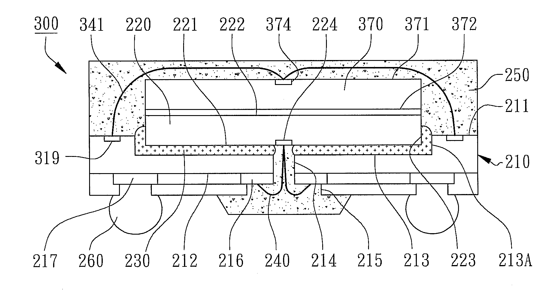
[0017]Please refer to the attached drawings, the present invention is described by means of embodiments below.

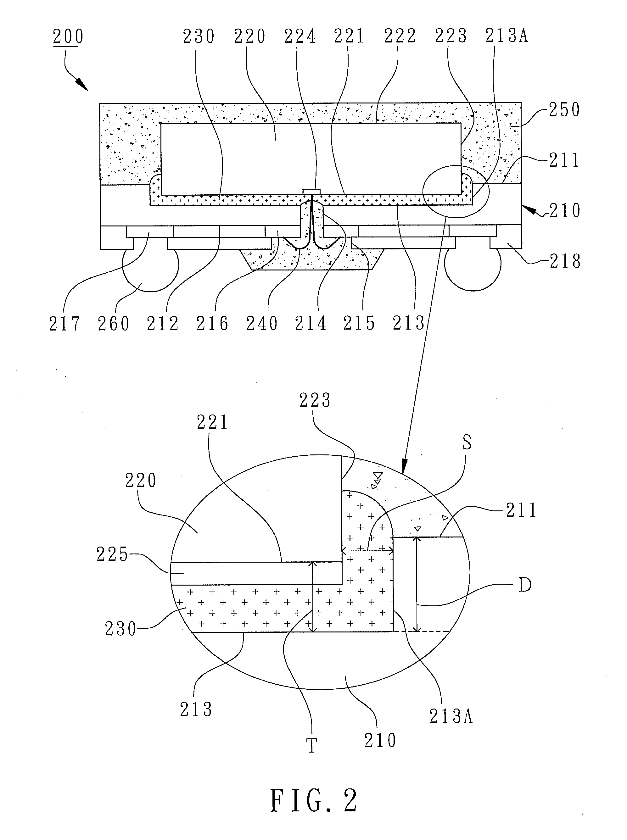
[0018]According to the first embodiment of the present invention, a WBGA semiconductor package 200 is illustrated in a cross-sectional view including a partially enlarged cross-sectional view of FIG. 2.

[0019]As shown in FIG. 2, the WBGA semiconductor package 200 primarily comprises a substrate 210, a first chip 220, a chip-bonding adhesive 230, a plurality of first bonding wires 240, an encapsulant 250, and a plurality of external terminals 260. The substrate 210 has an internal surface 211, an external surface 212, a depression 213 formed in the internal surface 211, and a slot 214 penetrating from the external surface 212 to the depression 213. The internal surface 211 is the surface of the substrate 210 without exposing from the encapsulant 250 for disposing the first chip 220 where the external surface 212 is the surface of the substrate 210 exposing from the encapsulant...


PUM


Abstract

A WBGA semiconductor package primarily comprises a substrate, a chip, a chip-bonding adhesive, a plurality of bonding wires electrically connecting the chip and the substrate, an encapsulant to encapsulate the chip and the bonding wires, and a plurality of external terminals disposed under the substrate. The substrate has a depression for accommodating the chip-bonding adhesive and a slot for passing through bonding wires. The chip is partially embedded in the depression to dispose on the substrate. During the chip bonding step, the chip-bonding adhesive is confined in the depression in a manner to fill the gaps between the sides of the first chip and the inwalls around the depression to generate a non-planar adhering interface by partially covering the sides of the first chip. Therefore, the total package thickness is reduced, the delamination of the passivation layer and the fractures at the sides of the chip are avoided.

Description

[0001]The present invention relates to a semiconductor device, especially to a window BGA (Ball Grid Array) semiconductor package.BACKGROUND OF THE INVENTION[0002]Among many semiconductor packages, Window Ball Grid Array (WBGA) is a semiconductor package with a slot opened in a chip-carrying substrate for passing bonding wires through the slot to electrically connect the substrate to the chip where the chip is attached to the top of the substrate. Then external terminals such as solder balls are disposed on the bottom surface of the substrate for mounting to an external printed circuit board. However, when a chip is attached onto the substrate by either liquid-type or paste-type chip-bonding adhesives, the chip-bonding adhesives become flowing due to raised temperatures and exerted pressures during the chip bonding processes leading to bleeding where the chip-bonding adhesives may bleed to bonding pads leading wire bonding failure. Therefore, the existing WBGA semiconductor package ...

Claims


Application Information

Patent Timeline
Patent Type & Authority Applications(United States)
IPC IPC(8): H01L23/49
CPCH01L23/3128H01L24/32H01L24/48H01L24/83H01L24/85H01L24/92H01L25/0657H01L2224/27013H01L2224/32014H01L2224/32145H01L2224/32225H01L2224/48091H01L2224/48227H01L2224/4824H01L2224/73215H01L2224/83051H01L2224/83192H01L2224/8385H01L2225/0651H01L2924/01005H01L2924/01013H01L2924/01029H01L2924/01075H01L2924/01079H01L2924/01082H01L2924/078H01L2924/07802H01L2924/15153H01L2924/15165H01L2924/15311H01L2924/01033H01L2924/014H01L24/29H01L2224/73265H01L2224/85H01L2224/06136H01L2924/00014H01L2924/00H01L2924/3512H01L2924/00012H01L2924/351H01L2924/15787H01L24/73H01L2924/181H01L2224/45099H01L2224/45015H01L2924/207
Inventor CHEN, CHIN-TI
Owner POWERTECH TECHNOLOGY
Why Eureka
Try Eureka