[0006]It is an object of the present invention to provide a method of forming a diffraction grating and a method of fabricating a
distributed feedback laser diode in which, in the process of forming a diffraction grating using a nano-imprint technique, a good pattern with a small number of diffraction
grating pattern defects can be obtained, and no damage is caused to the substrate.
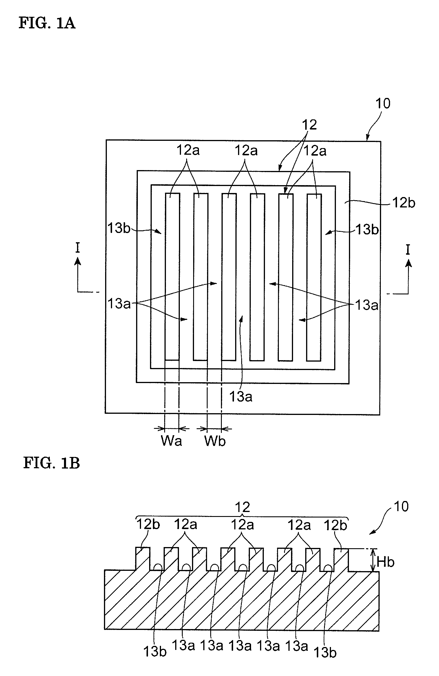
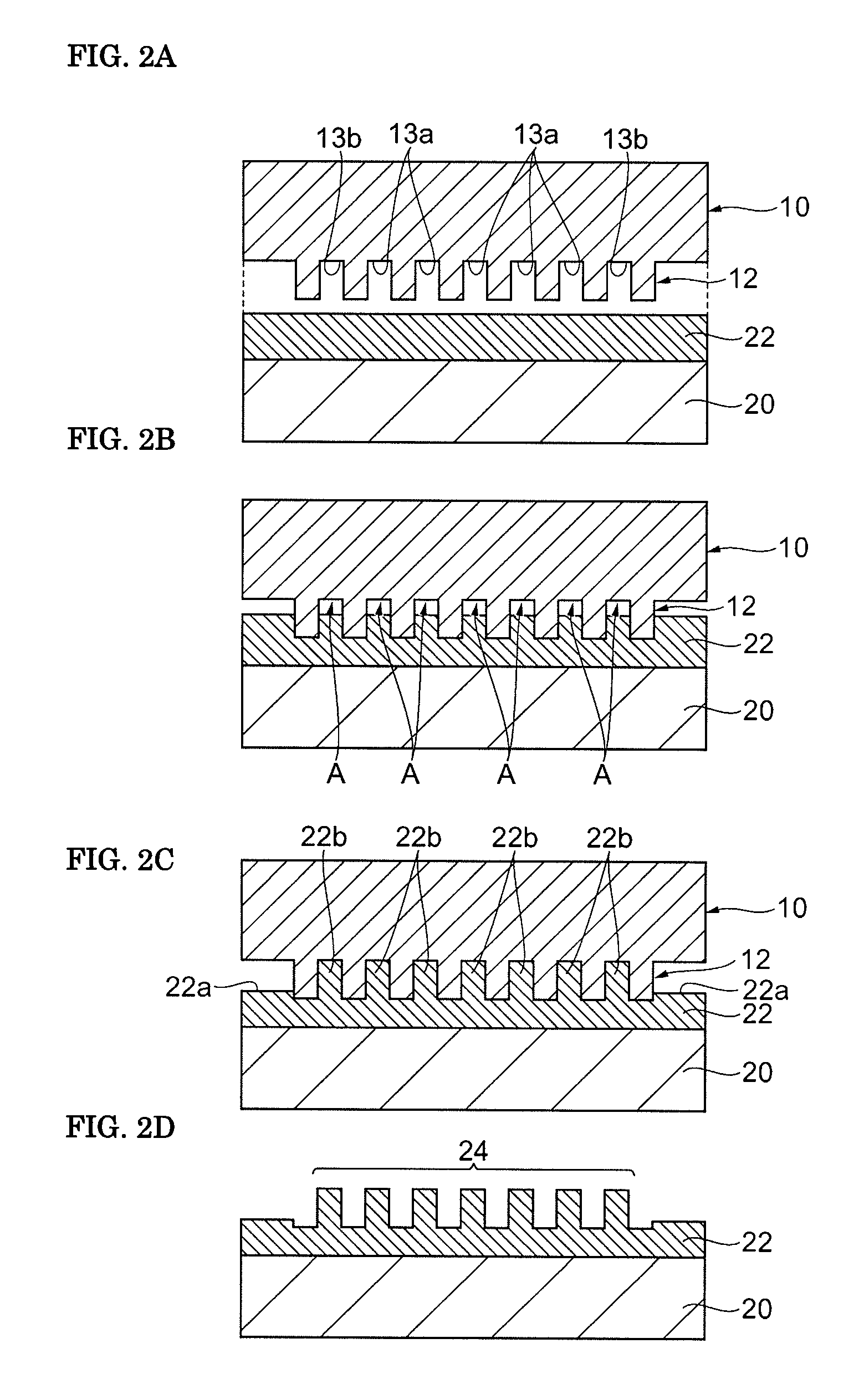
[0008]In the method of forming the diffraction grating described above, the projections and recesses of the mold are brought into contact with the resin layer in a chamber at a first pressure less than
atmospheric pressure. In this step, the recesses in the projections and recesses of the mold form a
closed pattern in the plane of the mold including the projections and recesses, and thereby, the space delimited by the recesses and the resin layer is kept in an airtight state. In the next step, the pressure in the chamber is set to a second pressure more than the first pressure in such a state by introducing a gas into the chamber. A portion of the resin layer not facing the projections and recesses is pressed by a
differential pressure between the first pressure and the second pressure, and portions of the resin layer having an airtight space between themselves and the recesses are sucked into the recesses. By such an action, even if the mold is not strongly pressed against the resin layer, the recesses of the mold are fully filled with portions of the resin layer. Consequently, by hardening the resin layer while maintaining such a contact between the resin layer and the mold, the pattern for the diffraction grating is accurately transferred and molded into the resin layer, and it is possible to decrease the number of defects of the pattern of the diffraction grating formed using, as a
mask, the resin layer having the pattern for the diffraction grating.
[0009]In the method of forming the diffraction grating, the resin layer may be composed of a
thermoplastic resin or a thermosetting resin. Preferably, the resin layer may be composed of an
ultraviolet (UV) curing resin. The
UV curing resin has a low
viscosity compared with other resins, such as a
thermoplastic resin. Therefore, when the resin layer is composed of the
UV curing resin, portions of the resin layer having an airtight space between themselves and the recesses of the mold easily move into the recesses. Consequently, the pattern for the diffraction grating can be more accurately transferred and molded into the resin layer, and thus the number of diffraction
grating pattern defects can be further decreased.
[0011]Furthermore, in the method of forming the diffraction grating, the
viscosity of the resin layer before being hardened may be 1.0 mPa·sec or less. By using the resin layer having such a low
viscosity, portions of the resin layer having an airtight space between themselves and the recesses of the mold become easily to move into the recesses. Consequently, the pattern for the diffraction grating can be more accurately transferred and molded into the resin layer, thus further decreasing the number of diffraction
grating pattern defects.
[0012]Furthermore, in the method of forming the diffraction grating, the second pressure in the chamber is an
atmospheric pressure. In such a case, the portion of the resin layer not facing the projections and recesses can be more easily and effectively pressed by the atmospheric pressure, and the recesses of the mold can be suitably filled with portions of the resin layer.
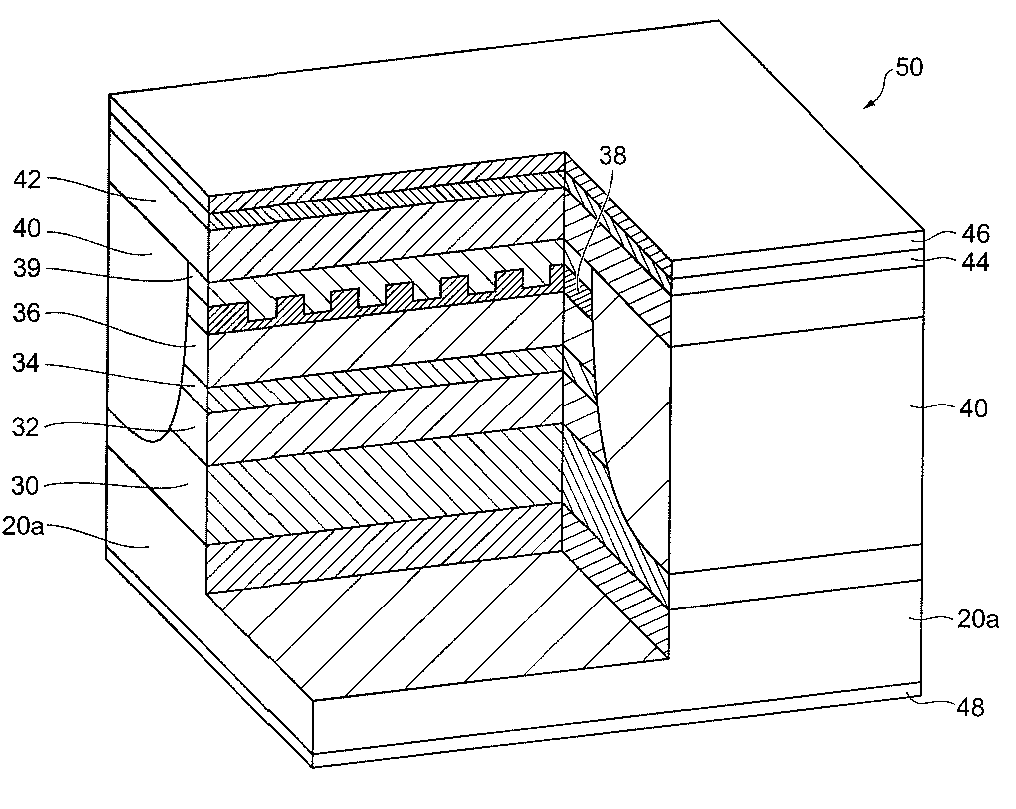
[0014]Furthermore, a method of fabricating a
distributed feedback laser diode according to the present invention includes a step of forming a resin layer on a
semiconductor substrate including an
active layer, a step of preparing a mold having projections and recesses for forming a diffraction grating, a step of bringing the projections and recesses of the mold into contact with the resin layer in a chamber at a first pressure less than atmospheric pressure, a step of setting a pressure in the chamber to a second pressure more than the first pressure while maintaining the contact, a step of hardening the resin layer while maintaining the contact between the resin layer and the projections and recesses so as to form a pattern for the diffraction grating on the hardened resin layer, and a step of forming the diffraction grating by
etching the
semiconductor substrate using the pattern for the diffraction grating. The recesses in the projections and recesses of the mold form a
closed pattern in the plane of the mold including the projections and recesses. According to such a method of fabricating a distributed feedback
laser diode, by the same action as in the method of forming the diffraction grating described above, a pattern for the diffraction grating can be accurately transferred and molded into the resin layer, and it is possible to decrease the number of defects of the pattern of the diffraction grating formed using, as a
mask, the resin layer having the pattern for the diffraction grating.

